An Analysis of SiC Power Electronics Implementation in Green Energy Based Extremely Fast Charging
(This article belongs to the Special Issue on Special Issue on Multidisciplinary Sciences and Advanced Technology 2022)
Export Citations
Cite
Deb, N. and Singh, R. (2022). An Analysis of SiC Power Electronics Implementation in Green Energy Based Extremely Fast Charging. Journal of Engineering Research and Sciences, 1(5), 231–242. https://doi.org/10.55708/js0105024
Naireeta Deb and Rajendra Singh. "An Analysis of SiC Power Electronics Implementation in Green Energy Based Extremely Fast Charging." Journal of Engineering Research and Sciences 1, no. 5 (May 2022): 231–242. https://doi.org/10.55708/js0105024
N. Deb and R. Singh, "An Analysis of SiC Power Electronics Implementation in Green Energy Based Extremely Fast Charging," Journal of Engineering Research and Sciences, vol. 1, no. 5, pp. 231–242, May. 2022, doi: 10.55708/js0105024.
Existing extremely fast charging (XFC) of electrical vehicles (EVs) is based on silicon power electronics and internal conversion of AC power into DC power. In this paper it has been shown that silicon carbide power electronics and the use of DC power source in the design of XFC of EVs has many distinct advantages over current XFC of EVs. Silicon carbide power electronics provide reduction of charging time, higher power conversion efficiency, size reduction of heat sink and improved battery’s state of health. The use of larger size silicon carbide wafers will further reduce the cost of power electronics based on silicon carbide. Use of green energy sources (solar and wind) and lithium-ion batteries for electrical power storage can provide end to end DC power network. Such networks combined with silicon carbide based XFC of EVs can play a revolutionary role in saving green electrical and provide reduced of charging of EVs. This paper reports almost 50% reduction in power losses by using Silicon Carbide DC technology. End to end DC power networks combined with SiC based XFC of EVs can play a revolutionary role in solving climate emergency.
1. Introduction
One of the most difficult problems faced by humanity is to solve climate emergency [1]. 24 % of the carbon emission globally is due to transportation as per 2018 data [2]. Among these, road vehicles contribute to 75% of transportation carbon emission [2]. Passenger vehicles contribute to 45.1% of this 75% and the rest come from heavy duty vehicles or freight vehicles [2]. According to 2019 data, 444 million metric tons of carbon dioxide was emitted by medium and heavy-duty trucks contributing to 18% of total global road freight CO2 emission [3]. Thus providing green electric power with highest efficiency of power utilization has the potential of providing solution to greenhouse gas emission due to surface transportation [4], [5]. For almost all over the world sustainable electric power can be provided by photovoltaics (PV) and battery based network at extremely-low cost, except where solar intensity is less than about 3-4 kWh/m2 per day [6]. In such places wind turbines can be major source of electrical power generation and PV can play the role of supplemental source of electrical power [6]. For automobiles, extremely fast chargers (XFCs) in the power range of 120-350kW are available in the market [2]. Medium/heavy duty trucks can use CharIN MCS charging standard under 1000V/1000A (1MW) today and have potential to use 1500V/3000A (4.5MW) in the future [5]. With advancements in technology and volume manufacturing of lithium ion batteries, the driving range of new battery electric vehicles (BEVs) has been steadily increasing and BEVs with over 700 miles range are in development stage [7]. However, one of the major roadblocks in the implementation of large scale electrification of surface transportation is the lack of low cost extremely fast charging (XFC) infrastructure. In a recent article [2] different aspects of current charging infrastructure has been reviewed by the authors and thus they concluded that the power electronics topologies are the cornerstone for charging stations. Creating XFCs more efficiently is the key to making the charging stations low cost and widespread [2]. In this paper improvement in XFC based on DC power and Silicon carbide power electronics has been analyzed. The previously reported literature in this area concentrates in the implementation of Silicon Carbide in EV hence enhancing the EV efficiency, but the implementation of SiC in charging technology remains rarely touched. The novelty of this paper is in the implementation of a new fully DC infrastructure powered by Silicon Carbide power electronics. In a recent review article [2] numerous publications dealing with various aspects of DC-SiC charging infrastructure has been examined by authors, which shows the limitation of previous research in this area. No concrete research is found in the heat loss, charging time reduction or a comparative study between Si or SiC power electronics in EV charging infrastructure. Most of the previous research focuses on the topology selection or particular methodology for heat loss reduction using SiC. A complete system level overview remains untouched in literature. Thus, the objective of this paper is on evaluating a system for XFC, based on end-to-end DC power and Silicon carbide power electronics. Thus providing green electric power with highest efficiency of power utilization has the potential of providing solution to greenhouse gas emission due to surface transportation [4][5]. For almost all over the world sustainable electric power can be provided by photovoltaics (PV) and battery based network at extremely-low cost [8-11], except where solar intensity is less than about 3-4 kWh/m2 per day [6]. In such places wind turbines can be major source of electrical power generation and PV can play the role of supplemental source of electrical power [6].
The paper is organized as follows; section 2 discusses the importance of a fully DC power system for charging infrastructure. In section 3, the importance of SiC based power electronics is described. Model developed in this paper is described in section 4. Validation of the model is described in section 5. Charging time calculations are described in section 6. The heatsink size for SiC and the reduction from its Si counterpart is described in section 7. Potential cost reduction pathway for SiC power electronics manufacturing is discussed in section 8. In section 9 paper has been concluded.
2. Importance of DC Power Charging Infrastructure for XFC
Thomas Edison conceptualized the fundamentals of locally generated DC power thus saving the transmission losses. But since the inception of power transmission, globally the electricity infrastructure is dominated by AC power. The situation is different today. More than 30% of power and capital can be saved by implementing DC instead of current AC based network [12]. Solar photovoltaics generates power in DC form, so does wind energy in erratic AC form that is converted to DC before AC transmission. Batteries and fuel cells store DC power. Due to lower cost of photovoltaics and batteries, high voltage DC (HVDC) transmission is playing a key role in the use of green electric power at the scale of 10.5 GW [13].
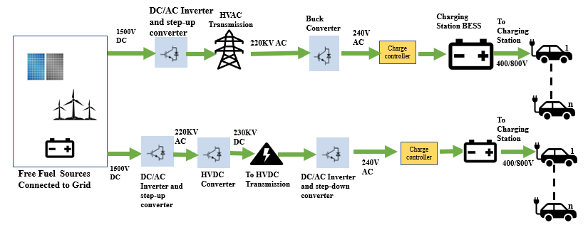
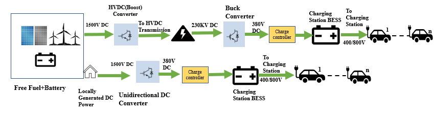
As shown in Figure 1, for charging electrical vehicles, the green electrical power generated by solar and or wind and stored in batteries is wasted in several DC to AC and AC to DC conversion steps in current high voltage AC (HVAC) transmission. Even for existing HVDC transmission illustrated in Figure 1, the DC power is first converted to AC power and then converted back to DC power. These unnecessary power conversion steps can be avoided in present day power generation and storage sources. As depicted in Figure 2, the green DC power is fed to both HVDC network and locally generated LVDC network and fJeeding the power to charging stations. As compared to Figure 2, the losses in Figure 1 are higher as inverter losses are higher and DC/DC conversion losses are lower to be discussed in the model derived in the next sections.
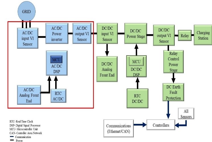
As depicted in Figure 3, the components shown in blue color, convert AC power into DC power, within current DC fast chargers. Thus wastage of a significant amount of green electrical power and capital is taking place in current charging stations. As opposed to this, if the components used as marked in the blue boxes in the AC system are eliminated, a large amount of electric power and capital can be saved if the entire charging infrastructure is based on DC power.
3. Silicon Carbide Based Power Electronics for Charging Infrastructure
In the last several decades, silicon power devices have dominated the world of power electronics. A large amount of energy is dissipated during conversion steps of AC/DC/AC due to the low electro thermal conductivity of silicon devices. High breakdown voltage, high operating electric field, high operating temperature, high switching frequency and low losses are several compelling advantages of silicon carbide power devices. It is suitable to use SiC devices in high voltage applications with the output capacitance being low. Thus, the magnetizing parts like transformers, chokes and inductors etc. are also reduced in size or completely eliminated. Packaging density becomes higher as the cooling requirement reduces. The use of SiC power electronics will reduce the dissipated energy, and the device life expectancy will increase due to less thermal exposure. As compared to silicon power electronics cost will be saved in two ways. SiC based power electronics will reduce the losses incurred in EV charging and also reduce the footprint of XFCs. As the cooling need decreases and power density increases, it will also significantly reduce the charging time [15]. By increasing packaging density the voltage capacity of EV can be doubled [16], hence similar technology can also be implemented in charging infrastructure. It also drastically reduces the size of the on board charger as reported in reference [17]. The fundamental limits of silicon power electronics can be overcome by the utilization of silicon carbide ICs in place of silicon ICs. Silicon carbide modules are providing higher power density of motor drive of electric vehicles [18]. Thus by enhancing the performance and cost reduction of power train of EVs and XFC, silicon carbide power electronics has the promise of accelerating growth of electrification of transportation.
4. Model
In this section the analytical model for power loss calculation has been developed. The calculated values of power loss of Si and SiC devices are compared with the best experimental data available in the literature.
4.1. Methodical Loss Calculation at Device Level
To calculate the power losses, Si and SiC devices with similar voltage level has been. The Si device is Digi chip N channel MOSFET 2SK2044 [19]. The SiC devices are Infineon F4-11MR12W2M1_B76 [20] and UnitedSiC UF3C170400K3S [21]. Two different SiC MOSFETs are used to show the potential of upcoming technology and will be referred to as SiC 1 and SiC 2 respectively. Infineon F4-11MR12W2M1_B76 is currently being used in high voltage PV and charging applications [14], whereas UnitedSiC is currently being used for Power Factor Correction (PFC) devices and have a potential for charging station applications as well. The parameters from datasheets are given in the Table 1.
Table 1: Parameters Used for Calculation
Symbol | Attribute | Si Digichip N channel MOSFET 2SK2044 [19] | SiC Infineon F4-11MR12W2M1_B76[20] | SiC UnitedSiC UF3C170400K3S[21] |
IDON | On Time Current | 4A | 100A | 14A |
RDSON | On Time Resistance | 2.4Ω | 14/18mΩ | 410mΩ |
tr | Rise Time | 15nS | 20nS | 13nS |
tf | Fall Time | 40nS | 28nS | 27nS |
VDD | Working Voltage | 600V | 1200V | 1700V |
D | Duty Cycle | 50% | 50% | 50% |
fsw | Switching Frequency | 1MHz | 1MHz | 100KHz |
toff | Off Time | 160nS | 67nS | 34nS |
MOSFET Power loss equations are taken from reference [22] and the values are calculated based on Vendor’s data sheet and application notes
Power loss during conduction or conduction loss is
$$P_{COND} = I_{D(ON)}^2 \ast R_{DS(ON)} \ast D\tag{1}$$
Where,
= Conduction loss
ID(ON)= On state current
RDS(ON) =On state Resistance
D= Duty Cycle
The switching losses are the sum of two separate losses viz ON time loss and OFF time losses given below. Energy loss during ON time,
$$E_{ON} = I_{D(ON)} V_{DD} \frac{t_{ri} + t_{f}}{2}
\tag{2}$$
Where,
EON=Energy Loss during ON time
ID(ON)= On state current
VDD= Drain Voltage
tri=Rise time
tf=Fall time
Therefore, the ON time power loss is given by:
$$P_{ON} = E_{ON} * f_{sw}\tag{3}$$
Where,
PON=ON time power loss
EON= ON time energy loss
fsw= Switching Frequency
Energy loss during OFF time,
$$E_{OFF} = \frac{I_{D(ON)} V_{DD} t_{off}}{2}\tag{4}$$
Where,
EOFF= Energy Loss during OFF time
ID(ON)= On state current
VDD= Drain Voltage
toff=off time
Therefore, the OFF-time power loss is given by,
$$P_{OFF} = E_{OFF} * f_{sw}\tag{5}$$
Where,
POFF=OFF time power loss
EOFF= Energy Loss during OFF time
fsw= Switching Frequency
Therefore total power loss,
$$P_{loss} = P_{COND} + P_{ON} + P_{OFF}\tag{6}$$
Using these equations in the values of Table 1 and using the methods for loss calculation from [23], 11.5% device level losses for Si-MOSFET and 5.81% for SiC-MOSFET 1 and 5.67% for SiC MOSFET 2 is obtained. Silicon power electronics is a matured technology, and silicon carbide power electronics is evolving technology. Thus in future even lower losses in SiC transistors can be expected.
4.2. Analytical Loss Calculation of Inverter:
The overall performance of the AC power system is defined by various losses. Different modulation techniques are used in three level inverters to modulate the switches. Based on our review article [2], Neutral Point Clamped 3-Level Inverter (NPC-TLI) is the most efficient topology for renewable applications [2]. However here a notional system based on an analytical model has been created. As explained previously, the loss calculation in real world is dependent on factors solely varying system to system. This specific system which is a clear representation of a DC-SiC based charging system is calculated and calibrated according to the equations mentioned below.
The selection of modulation technique is important to achieve marginal losses in the output current and voltage waveform and decreased harmonic distortion. Several modulation techniques rule the power electronics research arena, however two predominant ones in industry are sine pulse width modulation or SPWM and Space vector pulse width modulation or SVPWM. To solve the positive half cycle of the output voltage in SPWM technique, the voltage drop across Si-MOSFET over a conduction period can be expressed [22] as follows.
$$P_{\text{Cond(MOSFET)}} = \frac{1}{2\pi} \cdot \frac{1}{T_s} \int_0^{\pi} V_D \, i_D t_{\text{MOSFET}} \, \text{dwt}\tag{7}$$
Where,
PCOND(MOSFET)=Conduction Loss
VD= Voltage drop over condution period
tMOSFET = ON time for the MOSFET,
iD=Current over conduction period
Ts =switching time of the device given by 1/fs [23].
The MOSFET switching losses during ON and OFF time can be given by,
$$P_{\text{Cond(MOSFET)}} = \frac{1}{2\pi} \cdot \frac{1}{T_s} \int_0^{\pi} V_D \, i_D t_{\text{MOSFET}} \, \text{dwt}\tag{8}$$
Where,
Psw= MOSFET switching loss during T(ON+OFF)
fsw= Switching Frequency
VDSON=MOSFET ON time voltage
IDSON=MOSFET ON time current
VDSOFF=MOSFET OFF time voltage
IDSOFF=MOSFET OFF time current
The diode loss for this topology is:
$$P_{C(\text{DIODE})} = V_F I_0 + \frac{R_F I_0^2}{1 – D}
\tag{9}$$
Where,
PC(DIODE)= Diode Conduction Loss
VF= Diode Forward Voltage
I0==Ideal diode Current
RF=Diode Forward Resistance
A three phase NPC inverter contains three legs known as phase a, phase b, phase c. From reference [2], if the topology each leg is studied, it can be observed that contains 4 MOSFETs and two clamping diodes. The same amount of losses are considered in each of the semiconductor devices situated in the same half of the inverter. Similarly in each leg it can be assumed that the MOSFETs to have same amount of losses and the diodes to have same amount of losses.
Thus, the conduction loss of Si NPC-TLI inverter in SPWM modulation is obtained as follow:
$$P_{\text{COND}} = 3 \left[ 2P_{C(\text{MOSFET})\text{UP}} + 2P_{C(\text{MOSFET})\text{DOWN}} + P_{C(\text{DIODE})\text{UP}} + P_{C(\text{DIODE})\text{DOWN}} \right]\tag{10}$$
For switching loss the equation can be given by,
$$P_{\text{SW}} = 3 \left[ 2P_{(\text{MOSFET})\text{UP}} + 2P_{(\text{MOSFET})\text{DOWN}} \right]\tag{11}$$
Where,
P(MOSFET)UP=Power Loss in Upper MOSFETs of leg
P(MOSFET)DOWN=Power Loss in Lower MOSFETs of leg
The power loss in the charging capacitor can be given by,
$$P_C = R_{ESRC} \left( \frac{\Delta I_{DC}}{\sqrt{3}} \right)^2\tag{12}$$
Where,
PC= Power loss in capacitor
RESRC = Equivalent series resistance for the capacitor.
IDC= Capacitor Current
The values from Table 1 and equations 1-6 can be substituted in equation 7-9.
The total loss is given by,
$$P_{\text{TOTAL}} = P_{\text{COND}} + P_{\text{SW}} + 2P_C\tag{13}$$
A 10.64% inverter loss was calculated, putting the values of Table 1 in equations 7-13 and the method mentioned in [23].
4.3. Analytical Loss Calculation of a Rectifier:
To supply DC power to the EV chargers, a three-phase full wave diode bridge rectifier can be employed. Three phase PWM rectifiers are preferred for grid connected applications. But for applications like this, a diode rectifier will be a cheaper and robust option where the source is supplying a fixed amount of load. The average output voltage is given by [22].
$$V_L = \frac{6}{2\pi} \int_{\pi/3}^{\pi/2} V_{mL} \sin(\omega t + 30) \, d\omega t\tag{14}$$
Where,
VL= Load voltage
VmL= Maximum load voltage
The average load voltage was calculated to be 95.4% of source voltage for SiC 1 and 96.1% for SiC 2, thus giving a 4.6% and 3.9% loss respectively in similar way as inverter [23].
4.4. Analytical Loss Calculation of DC-DC Converter:
For the case of Figure 2, a unidirectional DC-DC converter is used for converting the PV/Wind generated erratic power to amplified smooth DC power. Different approaches of converting that DC- to charging station can be taken the simplest one being, installing a unidirectional DC to DC converter that feeds power directly to the charging station as shown in Figure 2. Unidirectional converters are simple in design thus reducing system cost and power losses. Unlike dual active bridge converter as shown in Figure 1 for the AC counterpart, it does not need a transformer, making it lighter in design as well. For a national and international scenario such as this one it is scalable and perfect. The piecemeal loss calculation [22] is given below:
The Power loss in the inductor [23] is given by,
$$P_L = \frac{1}{T_S} \int_0^{T_S} R_{ESRL} \left(i_L^2(t)\right) \, dt\tag{15}$$
Where,RESRL=Equivalent series resistance for the inductor.
IL= Load current
Ts =switching time of the device given by 1/fs
The Power loss in the capacitor is given by
$$P_C = R_{ESRC} \left( \frac{\Delta I_L}{2\sqrt{3}} \right)^2\tag{16}$$
Where,RESRC=Equivalent series resistance for the inductor.
The loss occurred in diode
$$P_D = I_o V_D (1 – D)\tag{17}$$
Conduction loss in MOSFET is given by equation (1) and switching loss is given by,
$$P_{SW} = I_{DON}^2 \cdot R_{DSON} \cdot D + I_o V_D (1 – D) + R_{ESRL} I_0^2 + R_{ESRC} \frac{\Delta I_0^2}{12}\tag{18}$$
(Variables are of the same interpretation as previous equations.)
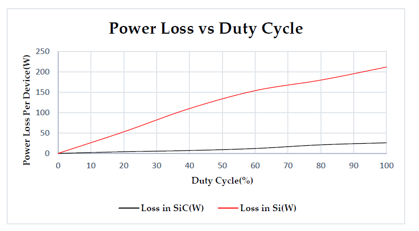
Duty cycle is directly proportional to power dissipation and 50% was decided to be optimum for this application. Reference [24] sheds more insight on this issue. For Silicon device the loss at 50% duty cycle was found to be 160W in terms of total losses. For SiC it was 10W per device. It is consistent with the loss data reported in section 7. Taking into consideration the duty cycle of 50%, input of 1200V for SiC 1 and 1700V for SiC 2 and load resistance of 17 mΩ and 410 mΩ respectively, the losses calculate to be 8.3% and 7.81% respectively. Here a fixed duty cycle has been chosen for comparison, as shown in Table 1. Power loss with varying duty cycle for SiC and Si power electronics is shown in Figure 4.
5. Model Validation:
Charging time data calculated by the model developed in this paper are compared with the experimental data reported in the literature for Si [24] and for SiC [25] based XFCs. As shown in Table 2, excellent agreement is observed between our calculated values and the experimental values.
6. Charging Time Calculations of SiC Power Electronics Based XFC:
Today XFC is recommended only a limited number of times to protect battery health. On the other hand fast charging is required for long-distance travel automobiles and is the only solution to electrify transportation of long-distance heavy-duty vehicles. In this section the charging time reduction, improved battery health and power system loss reduction with the implementation of SiC power electronics will be discussed. Higher efficiency of the power electronics provides lesser stress on battery and powertrain [25].
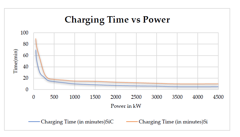
Table 2: Charging Time Reduction Comparison with Literature
Vehicle | Pack Voltage (V) & Approximate Energy kWh | Max Charging Power kW | |||||||||||
Range (mi) | Si XFC from Ref[24] (mins) | Our Si XFC model(mins) | SiC XFC from ref [25] (mins) | Our SiC XFC Model | |||||||||
Tesla Model 3 long range | 400 & 78.3 | 350 | 250 | 28 | 23 | 20 | |||||||
Porche Taycan Turbo S | 800 & 93.4 | 200 | 270 | 22.5 | 18 | 18.7 | |||||||
Xpeng EV | 800 & 250 | 125 | 480 | – | 5 | 4.5 | |||||||
ABB terra HP | 400 & 150 | 200 | 350 | 20 min | 17.5 | 15 | |||||||
To reduce charging time, battery pack voltage is increased to obtain maximum charging power and comes with additional complexity of a larger BMS. To accommodate the higher voltage, the number of cells connected in series must be increased. As an example, twice the number of cells must be connected in series for an 800V SiC based XFC as compared to the 400V Si based XFC. Additional circuitry like current sensors, controllers and temperature sensors etc. remain practically unchanged. The charging time also depends on the ambient temperature and circuit’s heat dissipation capacity [26]. Figure 5 shows the results of charging time as a function of power with Si and SiC based power electronics as the variable. An ambient temperature of 25°C was assumed. As observed from Figure 5, a steep decline in time is noticed up to 1MW, thereafter the heat loss increases and charging time get affected by the losses, and hence the time reduces less drastically than observed at the lower wattage.
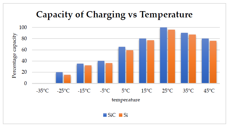
Figure 6 shows the capacity of charging at different ambient temperature for Si and SiC based XFCs. A standard high power battery pack of 1.2 MW was considered. As observed, the capacity of charging is very low at lower temperatures and is maximum at 25°C. At all temperatures, the capacity of charging is higher for SiC XFC.
Connecting a greater number of cells to operate at a higher power level comes with the drawback of deteriorated state of health (SOH) of batteries. The improvement of battery health while using SiC based fast charging is achieved by lesser heat exposure and better temperature control. The losses in Li-ion battery can be classified into two major types viz cycle life loss and calendar life loss. Overcharging the battery contributes the loss of cycle life. As an example if a 1.2 MWh battery is supposed to have 2000 cycles as per datasheet and if the charge is controlled to 1.1 MWh, then it is possible for the battery to last 2500+ cycles [27]. Calendar life loss is defined by the loss of health in battery after storing energy for typically 6-10 months [27]. A semi empirical formula for total loss [28] is given below.
$$Q^{\text{total loss}}(\delta t) = B_1 e^{B2 I_{\text{rate}}} I_{\text{rate}} \delta t + 0.5 f e^{-Ea / RTb} \, t^{-1/2} \delta t$$
Here B1 and B2 are the polynomials of the temperatures of the battery Tb. Irate is the rate of current for charging the battery and R is temperature coefficient. Therefore the model is highly temperature dependent. When the total loss is calculated over a period using different scenarios of DC power based XFC, the increase in battery health is observed. An energy dense battery of 1.2MWh is used in calculations in this paper. Table 3 shows the state of health (SoH) data for both Si and SiC based XFC.
Ambient temperature has a direct impact on the performance and reliability of lithium-ion batteries (LIBs). Battery capacity and cycle life are affected by operating temperature. Ideal operating temperature for Li-ion batteries is 15-35°C [26]. In general the useful life of LIBs can range between 3,000 to 5,000 cycles [29]. However, with optimal charging, the useful life can be up to 7,000 cycles [29]. Operating at higher temperatures will reduce cycle life due to cell degradation [30]. Continuous operation at higher than 35°C (95°F) will typically reduce battery cycle life by 50% [31].
Table 3: SOH with Age in Time Varying DC XFC Usage for Si and SiC Power Electronics Enabled Battery Energy Storage System
State of Health (SoH) (%) with Time Varying DCFC Use | Battery Age | |||||
Never | 0-3/Month | >3/Month | (Months) | |||
Si | SiC | Si | SiC | Si | SiC | |
1 | 1 | 0.95 | 1 | 0.92 | 0.956 | 3 |
0.95 | 0.97 | 0.89 | 0.94 | 0.85 | 0.91 | 6 |
0.92 | 0.95 | 0.85 | 0.915 | 0.82 | 0.89 | 12 |
0.88 | 0.91 | 0.82 | 0.89 | 0.79 | 0.865 | 24 |
0.85 | 0.88 | 0.79 | 0.87 | 0.765 | 0.85 | 36 |
0.83 | 0.86 | 0.76 | 0.855 | 0.73 | 0.845 | 48 |
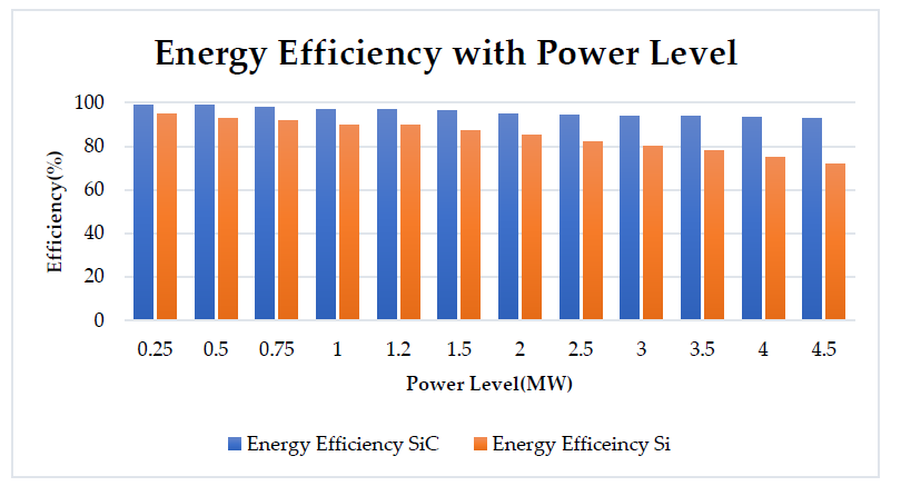
Figure 7 shows the energy efficiency as a function of power level both for Si and SiC based XFC. It is clearly evident from Figure 7 that at a higher power level, the fluctuations in energy efficiency are far lower in case of SiC than the corresponding values for Si. The efficiency almost decreases 20% at higher power levels for Si but remains in the range of 5% for SiC counterpart. This will not only reduce the loss in generated power but in addition will help battery health, powertrain health and the associated control equipment to operate at a stable operating condition.
7. Heat Sink Size Reduction
As shown in Figure 1, currently AC electricity infrastructure is used to provide charging of EVs which is based on silicon power electronics. To calculate the size of heat sink, first the system losses are calculated. The analytical model described in section 4 is used to calculate the losses of two SiC modules. The subsequent losses and the comparison with silicon counterparts [32] is given in Table 4.
Table 4: Charging Time Reduction Comparison Using SiC Counterparts
Conversion Level | % Loss reported in Silicon Devices [28] | %Loss derived for SiC1 | %Loss derived by SiC2 |
Inverter | 15 | 10.64 | 10.64 |
Rectifier | 6.1 | 4.6 | 3.91 |
Chopper | 9.2 | 8.3 | 7.81 |
After calculating the percentage losses of inverter, the heat sink has to be designed based on the available system parameters. But the more universal approach is to calculate the heat sink per module as explained below.
There is one heat sink solely responsible for inverter bank and another one responsible for the rectifier bank. For SiC XFC based on DC power as input, only one heat sink is necessary for DC-DC converter bank. For this paper three devices were used. Upcoming SiC technology of reference [21] was considered although the switching frequency was lower, but the potential for improvement was observed as a charging time reduction was calculated. To show the advantages of SiC system, a quantitative power loss analysis is performed based on the parameters of Table. 1. In the calculations, the switching loss of diode is neglected, because it is much smaller compared to the switching loss of IGBT or MOSFET. The sinusoidal pulse width modulation (SPWM) is employed in the control of inverter. Although different devices are used in the two systems, the calculation methods are identical. This method is applicable for any system size. The AC-DC and the DC-AC conversion stage can be designed in two ways. A solo inverter with high power rating equipment or an inverter bank with multiple inverters is connected. The later approach has been used for high power applications for reasons such as scalability of the system, ease of construction and carrying load, safety concerns and load sharing, and in case of fault in one inverter the rest of the bank can carry on the load.
Table 5: Heat Losses at Different Stages
Inverter Losses for Si- MOSFET | |
Conduction loss (per device) | MOSFET 70 W |
Diode 10 W | |
Switching loss (per device) | 80 W |
Total loss (6 MOSFETs+6Diodes) | 960 W |
Efficiency | 89.36% |
Total Losses | 960W |
Output Power | 9.02kW |
Rectifier Losses | |
Diode Conduction Loss | 10W |
Total Loss | 60W |
Efficiency of Bridge Rectifier | 95.4% |
Output Power | 8.96kW |
Therefore, in this section the heatsink design for each of the segments of inverter and rectifier banks will be calculated and compared to similar DC-SiC bank. A scaled down version is used here for practical dimension purposes as available in industrial datasheets. The system mentioned in this paper is massive, and no vendor has yet provided a datasheet for such design of a heat sink. Undoubtedly, if the system is stressed and made larger for XFC charging of high-power vehicles, the banks can be added together to operate smoothly. So a heatsink capable of removing 1,020W of heat must be selected. Reference [32] uses an identical system for 1800W heat loss. Selected heatsink was based on similar criteria.
Table 6: Heat Sink Calculation for Inverters
Table 6: Inverter Heat sink | Inverter heat sink |
Power Loss (Per Device) | 160W |
Efficiency | 89.36% |
Package size (Calculated from datasheet) | 170mm2 |
Heat Sink Size | Width(WD)= 300 mm, Depth (D)= 100 mm, Height (H)= 40 mm |
Heat Sink Weight | 3.6Kg |
Thermal Resistance Rheatsink | 0.021°C/W |
A smaller heatsink is required for rectifier as follows:
Table 7: Rectifier Heat Sink Parameters
Rectifier heat sink with SiC 1 | Rectifier heat sink with SiC 2 | |
Power Loss (Per Device) | 10W | 12.1W |
Efficiency | 95.4% | 94.5% |
Heat Sink Size | WD=50mm,D=20mm,H=15 mm | WD=55mm,D=22mm,H=15 mm |
Heat Sink Weight | 0.6Kg | 0.73Kg |
Thermal Resistance Rheatsink | 0.021°C/W | 0.0196°C/W |
For DC-DC converter one SiC MOSFET and one diode is used in the system constituting 8.3% of losses. So for a similar sized bank the losses will be half of the total rectifier and inverter bank. Hence the heatsink size will be half as well. But SiC has better power handling capability and the number of devices used in the circuit is lesser. The voltage level shown in Figure1 and 2 are 1500VDC- 220KV for inverter and 1500V to 380V for unidirectional rectifier / DC-DC converter. In both cases the number of devices is same. Using these numbers, SiC-MOSFET DC-DC converter heatsink is 28.6 % that of the inverter plus rectifier bank. But there are additional negligible losses. So a 30% round up number was estimated. An exact precise number in this scenario did not seem reasonable as every system will have different components. Using the new upcoming technology of SiC 2, slight increase in heat was observed due to higher RDS (ON), yet it was 44% of the size of the inverter plus rectifier bank in a Si counterpart.
After reducing the dissipated heat at component level, heat pump can be used to further reduce the size of the heat sink. In case of Tesla model Y [33], a heat pump is used to collect the dissipated heat from battery energy storage (BESS) and converter bank to heat or cool the car. For heating below -10 0C this method is highly effective [34]. The system efficiency is improved by a liquid cooled condenser where the BESS and converters reject heat and it’s moved around in passenger cabin, battery, and the drive unit and sometimes outside ambient temperature to improve system efficiency [35]. The sizing of heat pump was a critical aspect [36] to determine the overall cooling system size reduction. Almost 7-30% heat is recycled using this technology depending on the outside ambient temperature [33].
A similar technology for XFC heat reduction is proposed in this paper. The residue heat from the converters may be compressed and used to heat or cool the adjacent control rooms or used for other purposes. Calculating the correct size of heat pump is imperative to ensure the heating technology is not dissipating too much heat while propagating through the pump. Several factors like the kilojoules needed for the space, the direct sunlight exposure of the recipients, the energy rating of the heat pump etc. are important factors to be considered while calculating the heat pump size [36]. By accurately calibrating the dimensions, Tesla was able to make their heat pump 300% more efficient than their resistive heating system [37]. Since the system size for a charging station is larger than that of a vehicle, the dissipated heat during propagation should be higher. The recalibrated heat sink values for different level of converters using both SiC and heat pump are given in Table 8.
Table 8: Heat Sink Dimensions Calibrated for Each Converter Bank after Installing Heat Pump and Implementing SiC Technology
Converter Bank | Heat Sink Size |
Rectifier Bank | WD=20 mm, D= 10 mm, H= 5 mm |
Inverter Bank | WD= 70mm, D= 50mm, H=10mm |
DC-DC Converter Bank | WD= 30mm, D= 20mm, H=10mm |
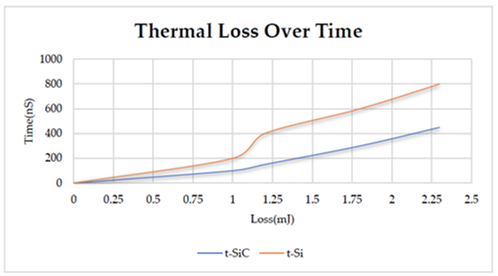
Assuming constant current, the thermal loss over operating time was calculated with the given RDS(ON) and the standard circuit heating formula H= I2Rt. These results are shown in Figure 8 both for Si and SiC based XFC.
8. Manufacturing Cost Reduction of Silicon Carbide Power Electronics
The cost of SiC based power electronics can be significantly reduced in very near future, it is pretty evident [38]. Attributable to the high growth of EVs, Silicon carbide modules are providing higher power density of motor drive of electric vehicles [39]. No supply-chain issues in the manufacturing of its related power electronics are predicted due to the abundance of elements of SiC. Higher performance, higher reliability, higher yield, and lower cost of ownership of SiC based power electronics will be provided if policies in favor of electrification of transportation, volume manufacturing, single wafer processing [40] and large diameter wafer manufacturing are implemented [41]. Silicon carbide fabs are migrating from 150 mm wafers to 200 mm wafers [42]. With progress in technology, the feature size of transistors and defect density will also be reduced. Akin to Si, the cost of SiC power electronics with the use of 300 mm SiC wafers will further reduce. Reminiscent of the growth of Si based nanoelectronics and power electronics, the growth of SiC based power electronics is expected to evolve in a similar fashion. Recently, the author of Reference [43] has analyzed the current and projected cost of silicon carbide die.
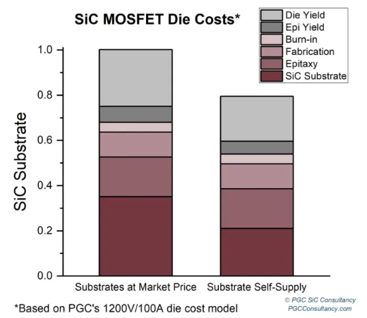
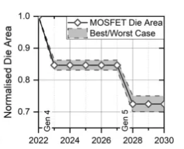
As shown in Figure 9 [43], companies having in-house manufacturing of SiC wafers have the advantage of lower cost of SiC die. Based on industrial trends, the author of reference [43] has also projected the substrate cost, defect density, die size and die cost reduction from current values to year 2030. Due to current geo-political event, we expect that the electrification of transportation will accelerate and the graphs shown in Figure 10, may even reduce faster than projected in reference [43]. converters and high voltage DC to medium voltage DC converters that can provide 100 % DC power for EV charging infrastructure [44]. Other markets such as power networks, high frequency, and ultra-high-power electronics for harsh environments etc. will also progress with the success of SiC power electronics. The lower cost of SiC based XFCs will contribute to the growth in other markets as well.
9. Conclusions:
In this paper the design and analysis of XFC based on silicon carbide power electronics has been provided. As compared to Silicon power electronics based XFC, reduction of charging time, higher power conversion efficiency, reduced size of heat sink, and improved battery state of health are obtained in case of SiC power electronics XFCs. For heavy duty trucks SiC based XFC may be the only practical solution. The use of larger diameter silicon carbide wafers will further reduce the cost of SiC based power electronics. Using free fuel energy sources namely solar and wind and the use of lithium ion batteries for electrical power storage, it is possible to implement end-to-end DC system for power generation, power storage, power transmission and power distribution. Combining such DC power network and SiC based DC power XFC will provide revolutionary solution for electrification of transportation.
The use of silicon carbide-based power electronics will also be enabler of medium voltage DC to high voltage DC
Nomenclature
AC- Alternating Current
BMS- Battery Management System
BESS- Battery Energy Storage System
CHAdeMO- Charge de move
CharIn- Charging for Megawatt systems
CPS- Cyber Physical System
DAB- Dual Active Bridge
DC- Direct Current
ECU- Electronic Control Unit
EOT- Electrification of Transportation
ESU- Energy Storage Unit
EV: Electric Vehicle
EVCS- Electric Vehicle Charging Station
HVAC- High Voltage Alternating Current
HVDC- High Voltage Direct Current
ICEV- Internal combustion Engine Vehicle
IGBT- Insulated Gate Bipolar Transistor
kW- Kilowatt
LIB- Lithium-Ion Battery
MCS-Megawatt Charging System
MOSFET- Metal oxide semiconductor field effect transistor
MVAC- Medium Voltage Alternating current
MW- Megawatt
NPC-TLI- Neutral Point Clamped 3-Level Inverter
PFC-Power Factor Correction
PV- Photovoltaic
PWM- Pulse Width Modulation
RES- Renewable Energy System
SiC- Silicon Carbide
SoC- state of charge
SoH- State of Health
THD- Total harmonic distortion
XFC: Extremely fast charging station
- Facts about the climate emergency, Available Online: https://www.unep.org/explore-topics/climate-action/facts-about-climate-emergency
- N. Deb, R.Singh, R.R Brooks, and K.Bai, 2021. A Review of Extremely Fast Charging Stations for Electric Vehicles. Energies, 14(22), p.7566.doi.org/10.3390/en14227566
- H. Ritchie,” Cars, Planes, Trains: Where do CO2 Emissions from Transport Come From”, October 16, 2020 https://ourworldindata.org/co2-emissions-from-transport
- Volume of medium and heavy-duty truck greenhouse gas emissions in the United States from 1990 to 2019, Available Online: https://www.statista.com/statistics/1120519/us-med-heavy-trucks-vehicle-ghg-emissions/
- Monthly mw+ multi-port charging meeting Available online: https://anl.app.box.com/s/webuku4bbbfbrbryqx62rr44fr8zrlck
- R. Singh, G.F. Alapatt, and G. Bedi, 2014. Why and how photovoltaics will provide cheapest electricity in the 21st century. Facta Universitatis, Series: Electronics and Energetics, 27(2), pp.275-298.
- Tesla Model S gets 752 miles of range with ONE’s new energy-dense battery pack, Available https://electrek.co/2022/01/05/tesla-model-s-752-miles-range-one-energy-dense-battery-pack/
- M. Roser, “Why did renewables become so cheap so fast?” Our World in Data, Dec. 01, 2020. [Online]. Available: https://ourworldindata.org/cheap-renewables-growth
- S. Pires, “The IEA Announces Solar Power Is Now the Cheapest Form of Energy,” My Modern MET, Nov. 3, 2020. [Online]. Available: https://mymodernmet.com/solar-power-cheapest-energy/
- J. Shah, https://pv-magazine-usa.com/2021/04/12/saudi-arabias-second-pv-tender-draws-world-record-low-bid-of-0-0104-kwh/
- https://cleantechnica.com/2021/11/13/solar-pv-pvstorage-costs-keep-dropping-new-nrel-reports-show/
- Singh, and K. Shenai, ,” DC Microgrids and the Virtues of Local Electricity”, IEEE Spectrum, on Line, Posted 6 Feb 2014 |
- Submarine cable to connect 10.5 GW wind-solar complex in Morocco to the UK grid, Available Online: https://www.pv-magazine.com/2021/04/22/submarine-cable-to-connect-10-5-gw-wind-solar-complex-in-morocco-to-the-uk-grid/
- Deb, R. Singh, and H. Bai, “Transformative Role of Silicon Carbide Power Electronics in Providing Low-cost Extremely Fast Charging of Electric Vehicles,” 2021 IEEE Fourth International Conference on DC Microgrids (ICDCM), 2021, pp. 1-6, doi: 10.1109/ICDCM50975.2021.9504653.
- Vecca, “Benefits and Advantages of Silicon Carbide Power Devices over Their Silicon Counterparts”. http://www.semiconductor-today.com/features/PDF/semiconductor-today-apr-may-2017-Benefits-and-advantages.pdf
- Slovick, “800-V SiC Inverter Promises to Cut EV Charging Time in Half”. October 21, 2019 https://www.electronicdesign.com/markets/automotive/article/21808734/800v-sic-inverter-promises-to-cut-ev-charging-time-in-half
- Shepard, “SiC Enables EV Charger That is More Efficient & 10X Smaller”. October 19, 2018
- Silicon Carbide Modules Unlock Higher Power Density in Motor Drives, Silicon Carbide Modules Unlock Higher Power Density in Motor Drives – EE Times Europe
- Datasheet Si, available online: https://www.digchip.com/datasheets/parts/datasheet/413/2SK2044LS-pdf.php
- Datasheet SiC 1, available online: https://www.infineon.com/dgdl/Infineon-F4-11MR12W2M1_B76-DataSheet-v02_00-EN.pdf?fileId=5546d4627956d53f01797a3de84651f2
- Datasheet SiC 2, available online: https://unitedsic.com/datasheets/DS_UF3C170400K3S.pdf
- N. Undeland, W.P. Robbins, and N. Mohan, 1995. Power electronics. In Converters, Applications, and Design. John Wiley & Sons, Chapter6,7,29.
- MOSFET power losses and how they affect power-supply efficiency, available online: https://www.ti.com/lit/an/slyt664/slyt664.pdf?ts=1641473977604&ref_url=https%253A%252F%252Fwww.google.com%252
- Aghabali, J. Bauman et al 2020. 800V Electric Vehicle Powertrains: Review and Analysis of Benefits, Challenges, and Future Trends. IEEE Transactions on Transportation Electrification. DOI: 10.1109/TTE.2020.3044938
- XPeng Announces 480 kW Chargers And 800V SiC EV Platform, Available Online: https://insideevs.com/news/543306/xpeng-480kw-chargers-800v-platform/
- Lambert, “This Dumper Truck is the World’s Largest Electric Vehicle with a Massive 700 kWh Battery Pack”, September 17, 2017 https://electrek.co/2017/09/17/electric-dumper-truck-worlds-largest-ev-battery-pack/
- Keil, S.F. Schuster ,2016. Calendar aging of lithium-ion batteries. Journal of The Electrochemical Society, 163(9), p.A1872.)
- Richard, and M. Petit, 2018, June. Fast charging station with battery storage system for EV: Grid services and battery degradation. In 2018 IEEE International Energy Conference (ENERGYCON) (pp. 1-6). IEEE.) DOI: 10.1109/ENERGYCON.2018.8398744
- New Tests Prove: LFP Lithium Batteries Live Longer than NMC, https://www.onecharge.biz/blog/lfp-lithium-batteries-live-longer-than-nmc/
- “Grid scale battery storage”, Available Online: https://www.nrel.gov/docs/fy19osti/74426.pdf
- Gopal, and A. Eggert, “Clearing the Air: Yes. Batteries are Ready to Power Long-Range Freight Trucks”, January 21, 2021 https://www.forbes.com/sites/anandgopal/2021/01/19/clearing-the-air-yes-batteries-are-ready-to-power-long-range-freight-trucks/?sh=1a5dfa6d3494
- Zhao, J. Wang, A.Q. Huang, and A. Agarwal, 2007, September. Comparisons of SiC MOSFET and Si IGBT based motor drive systems. In 2007 IEEE Industry Applications Annual Meeting (pp. 331-335). IEEE. DOI: 10.1109/07IAS.2007.51
- Model Y is the first Tesla with a heat pump. Here’s why that’s a big deal, Available Online:.https://www.currentautomotive.com/model-y-is-the-first-tesla-with-a-heat-pump-heres-why-thats-a-big-deal/
- Tesla Model Y Heat Pump Details Infrequently Discussed By The Media, Available Online: https://insideevs.com/news/452464/tesla-model-y-heat-pump-system-details/
- “Elon Musk: Tesla Model Y heat pump is some of the best engineering I’ve seen in a while”, Available Online: https://electrek.co/2020/03/23/tesla-model-y-heat-pump-elon-musk-best-engineering/
- How to choose the right size heat pump, Available Online: https://www.hpac.co.nz/tipsandadvice/how-to-choose-the-right-size-heat-pump/
- Tesla Model Y Heat Pump: Deep Dive and Closer Look, Available Online: https://www.tesmanian.com/blogs/tesmanian-blog/tesla-model-y-heat-pump-range
- The right climate for efficient semiconductors, Available Online: https://www.ingenia.org.uk/ingenia/issue-78/semiconductors
- Fuertado, and D. Martin, “Silicon Carbide Modules Unlock Higher Power Density in Motor Drives,” EETimes, Nov.18, 2021. [Online]. Available: https://www.eetimes.eu/silicon-carbidemodules-unlock-higher-power-density-in-motor-drives/
- Singh, and R. Thakur, 2005. Chip making’s singular future. IEEE Spectrum, 42(2), pp.40-45. DOI: 10.1109/MSPEC.2005.1389515
- Singh, and A.A Asif, 2016. Ultra large scale manufacturing challenges of silicon carbide and gallium nitride based power devices and systems. ECS Transactions, 75(12), p.11. DOI:10.1149/07512.0011ecst
- The Silicon Carbide Race Begins, Available Online: https://semiengineering.com/the-silicon-carbide-race-begins/
- M. Emilio, https://www.powerelectronicsnews.com/sic-power-devices-lowering-costs-to-drive-adoption/
- R. Singh, P. Paniyil, and Z. Zhang,” Transformative Role of Power Electronics in Solving Climate Emergency”, IEEE Power Electronics Magazine (In Review)
No related articles were found.