Acceleration of Image Processing with SHA-3 (Keccak) Algorithm using FPGA

(This article belongs to the Special Issue on Special Issue on Multidisciplinary Sciences and Advanced Technology (SI-MSAT 2022) and the Section Telecommunications (TEL))
Export Citations
Cite
Sideris, A. , Sanida, T. , Tsiktsiris, D. and Dasygenis, M. (2022). Acceleration of Image Processing with SHA-3 (Keccak) Algorithm using FPGA. Journal of Engineering Research and Sciences, 1(7), 20–28. https://doi.org/10.55708/js0107004
Argyrios Sideris, Theodora Sanida, Dimitris Tsiktsiris and Minas Dasygenis. "Acceleration of Image Processing with SHA-3 (Keccak) Algorithm using FPGA." Journal of Engineering Research and Sciences 1, no. 7 (July 2022): 20–28. https://doi.org/10.55708/js0107004
A. Sideris, T. Sanida, D. Tsiktsiris and M. Dasygenis, "Acceleration of Image Processing with SHA-3 (Keccak) Algorithm using FPGA," Journal of Engineering Research and Sciences, vol. 1, no. 7, pp. 20–28, Jul. 2022, doi: 10.55708/js0107004.
In our digital world, the transmission of images between people has played an essential part in every cedures to ensure the integrity and accuracy of the communicated data are required. Today, hashing is the most popular and secure way. This article focuses on the SHA-3 for hashing images dimensions 256 256 pixels with our custom implementations on the FPGA based on the Very High Speed Integrated Circuit Hardware Description Language (VHDL). We perform our experiments on the Intel Arria 10 GX FPGA and the Nios II processor. Also, our experiments with calculating metrics such as entropy, NPCR and UACI show that the SHA-3 is secure, reliable and has high application potential for hashing images. We propose designs to improve throughput, security, and efficiency criteria. We strengthened our design using the IP Block Floating Point Hardware 2 (FPH-2). Our experiments with the proposed implementation have shown increased throughput by 14.38% and efficiency by 13.95% of the SHA-3 algorithm. Finally, we compared our findings to other researchers’ existing optimization methodologies, giving data that demonstrate our research’s strengths.
1. Introduction
As well as for any other transmitted information, the integrity of the image transfer is achieved via cryptographic hashing functions. An essential role in today’s world of digital transmissions plays cryptographic hash functions. It is an essential technology used to protect information integrity when information is transmitted over a grid. Nowadays, image information security is crucial, mainly in the army, meteorology, medicine, intelligent robots, commerce, etc. As a result, the cryptographic society’s mission has become the creation of an image hash feature [1]–[3].
Watermarking is the technique for guarding digital images and video against alterations or corruption. Hash features can be successfully used in range authentication and image watermark applications [4]. In expansion, a picture hash procedure would significantly simplify investigations. Moreover, hashing is utilized within comparisons in vast databases, in which a lot of similar arrangements of an image can exist [5].
In this paper, we developed and implemented the famous Keccak (SHA3-256) algorithm in the Intel Arria 10 GX FPGA board. We utilised the new algorithm SHA-3 with a 256-bits output size because it provides high safety and maintains the original image quality during the hash process. We provide a FPH-2-based approach in our tailor-made design. We compare the two strategies we have designed with other
similar models and with standard evaluation criteria (entropy, Unified Averaged Changed Intensity (UACI), Number of Pixel Changing Rate (NPCR), efficiency and throughput).
The main contributions of our work are:
- We suggest a novel two-stage pipelined design for the SHA-3 algorithm in 256 bits output length for 256 × 256 pixel images, optimizing FPGA devices’ acceleration and We have used SHA-3 with a 256-bits output length because it provides high security.
- We contribute an innovative procedure established on the FPH-2 element in our design, which delivers an inferior cycle count. We analysed the optimisation plan to maximise the throughput and efficiency measures, and at the same time, algorithm SHA-3 keeps the actual image quality.
The remains of the article are organized as follows: In the next Section 2, we introduce study works which are similar to ours. In Section 3, we outline our experiments in detail for the implementation of SHA3-256 (Keccak) in 256 × 256 pixel images on an Intel Arria 10 GX FPGA device. In Section 4, we show and discuss the testing results and the implementation evaluation of our work. Finally, in Section 5, we outline our study’s conclusions and future work.
2. Related work
From the literature review, we selected similar works for comparison. We chose the specific articles because they are up to date state of the art designs using the SHA-3 algorithm. The objective of all these models is to enhance performance while at the same period trying to decrease power consumption and area on the FPGA board.
An efficient and secured image encryption algorithm is proposed in [6], jointly using the SHA-3 hash function with two-dimensional Arnold chaotic maps. In the permutation step, a conventional encryption technique is described with four random shuffling rules to avoid time consumption in the pixel position index sorting phase. Numerical findings reveal that the proposed encryption technique may improve security and speed up the implementation of digital picture transmission.
On work [7], the authors focus on 256 × 256 grayscale image encryption. The implementation was done using VHDL. The results show that the proposed architecture for the SHA3-256 algorithm achieved a throughput of 35.593 Gbps, maximum frequency of 458 MHz, area (slices) 2.984 and efficiency of 11.92 Mbps/Slices.
The authors in [8] suggest a new implementation with a chaotic encryption algorithm for images in dual chaotic maps. The SHA-3 and an auto updating system calculate the hash values to construct a Logistic map’s control parameter and initial condition. Behind that, all the permutations are executed for rows and columns in an image to exchange pixels. As an effect, the presented algorithm can oppose known-plaintext attacks efficiently.
On work [9], the authors focus on all candidates in the SHA-3 competition in terms of their effectiveness in the area (slices). Their research was conducted with the Virtex-5 and Virtex-6 FPGA devices. The implementation was done using VHDL. Their architecture for the SHA3-256 algorithm achieved better results with the Virtex-6 device with a throughput of 1.071 Gbps, maximum frequency of 197 MHz, area (slices) 397 and efficiency of 2.69 Mbps/Slices.
The authors in [10] focus on all candidates in the SHA- 3 finalists in the FPGA. The main goal of the research is to analyze the performance of all candidates in terms of throughput and area. In their work, they used a Virtex 5 and Virtex 6 from Xilinx and Stratix III and Stratix IV from Intel and the implementation was done using VHDL. The re- sults show that the proposed architecture for the SHA3-256 (Keccak) algorithm achieves better results with the Virtex-6 device. They achieved a throughput of 16.236 Gbps, area (slices) 1.446 and efficiency of 11.23 Mbps/Slices.
In [11], the authors work on the assessment of all SHA-3 finalists in FPGA devices. The primary goal of their work is to compare all candidates with the evaluation criteria of throughput, clock frequency and area. Their research was conducted with Virtex-5, 6 and 7 FPGA devices. The implementation was done using VHDL. The results show that the proposed design for the SHA-3 algorithm achieves better results with the Virtex-5 device in clock frequency, region and performance than other candidates.
The authors in [12] deal with the performance implementation of all SHA-3 finalists in the FPGA. The main goal of the research is to provide a fair and comprehensive evaluation of all candidates in terms of throughput and area. Their work used a Xilinx Virtex-5 and Virtex-6 device, and the implementation was done using VHDL. Their architec- ture for the SHA3-256 (Keccak) algorithm with the Virtex-6 device achieved a throughput of 12.817 Gbps and efficiency of 10.08 Mbps/Slices, a maximum frequency of 282.7 MHz and an area (slices) of 1.272.
In [13], the authors investigated the calculatedly efficiency of all SHA-3 finalists in FPGA devices. The primary purpose of this study is to compare the efficacy of this de- sign in terms of fragmented functions per unit area. The work was done using a Virtex-5 FPGA chip with VHDL as the implementation language. The suggested design for the SHA3-256 (Keccak) algorithm requires 1.117 slices (area), reaches a maximum frequency of 189 MHz, and has a throughput of 6.263 Gbps and an efficiency of 3.17 Mbps/Slices, according to the results.
The authors in [14] deal with the effective implementation of all SHA-3 finalists in the FPGA. The main goal of the research is to provide a basic comparison between all candidates in terms of clock frequency, throughput and area. They used a Xilinx FPGA device in their work, and the implementation was done using VHDL. Their architecture for the SHA3-256 algorithm achieved a throughput of 11.9 Gbps, a maximum frequency of 215 MHz, and an area (slices) of 4.745.
On work [15], the authors suggested a pipelining archi- tecture for the SHA-3 algorithm in order to raise its efficiency and throughput of them. The proposed architectures were implemented in FPGA Virtex-2, Spartan-3 and Virtex-4 us- ing Verilog. According to the experimental findings, the suggested designs provide excellent performance with the Virtex-4 device in terms of total area, maximum frequency, throughput, and throughput/area.
All of these documents and many more [16]–[25], have as their main goal the increase of its throughput and efficiency metrics in the SHA3 (Keccak) algorithm. However, improved architecture is always needed to enhance through- put and efficiency. Compared to previous works, we de- signed and implemented two designs of the SHA3, using the Nios II/f processor. Our first design applies a two-stage pipeline architecture. The second concerns a method based on the FPH-2 part in a two-stage pipeline design. The two approaches we suggest in this paper deliver a secure SHA3 with 256bits hashing implementation. The proposed design with the FPH-2 component and the two-stage pipelined architecture outperforms existing implementations.
3. Implementation for Image Hashing
This section analyses all the design components we have im- plemented for the SHA3-256 (Keccak). In our experiments, we have used the Standard Edition (SE) Quartus II ver. 18.3 and the DE5a-Net board. Table 1 displays the specifications of the Terasic DE5a-Net board.
3.1. Nios II – Soft-Core Embedded Processor
The Nios II is wholly implemented in the FPGA. It is considered suitable for most embedded applications and provides flexibility for real-time and cost-sensitive functionality [26]. Nios II is offered in three different configurations: fast, standard and economy. The Nios fast is optimized for the most high performance; this performance can be modified using patronage instructions, hardware accelerators, and the highest bandwidth switch fabric. The Nios standard is used for increased performance, and Nios economy is appropriate for mediocre performance [27].
Table 1: FPGA Specifications
Parameters Values
FPGA id 10AX115N2F45E1SG
Board Terasic Intel Arria® 10 GX FPGA System Clock Frequency 50MHz Oscillator
Memory SO-DIMM 2400 MHz SDRAM 2x4GB DDR4
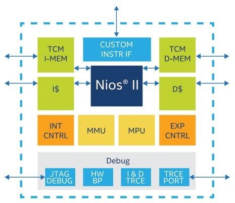
In our experimentations, we utilised the processor NIOS II/f, as shown in Figure 1. Its main characteristics are oper- ation with a 6-stage pipeline to gain the external interrupt controller, custom instructions, highest DMIPS/MHz and optional hardware multiply to improve arithmetic perfor- mance [28, 29].
3.2. Nios II Custom Instruction Implementation
Custom instructions provide us with the capability to feet the Nios II processor to complete the requirements of an application. A custom instruction logic block interfaces with the Nios II processor through 3 ports: dataa, datab, and result. The custom instruction obtains input on its dataa port and datab ports and drives the final results to its result port. A conduit interface to external logic provides a custom interface to method resources exceeding the Nios II pro- cessor. A custom combination statement complements its logical function in a single clock cycle. Custom multi-cycle instructions require two or more time cycles to operate. An extended custom instruction allows the implementation of several different operations. An Internal register file allows to access the Nios II for input or output or both [30].
Figure 2 shows a block graph with all ports of a Nios II custom instruction.
3.3. Floating Point Hardware 2 (FPH-2)
We may choose to avoid the floating-point divider because it takes more resources than other instructions. If Nios II does not employ floating-point division, we may choose to do so. We can rearrange our code in some cases to reduce or even eliminate separated processes.
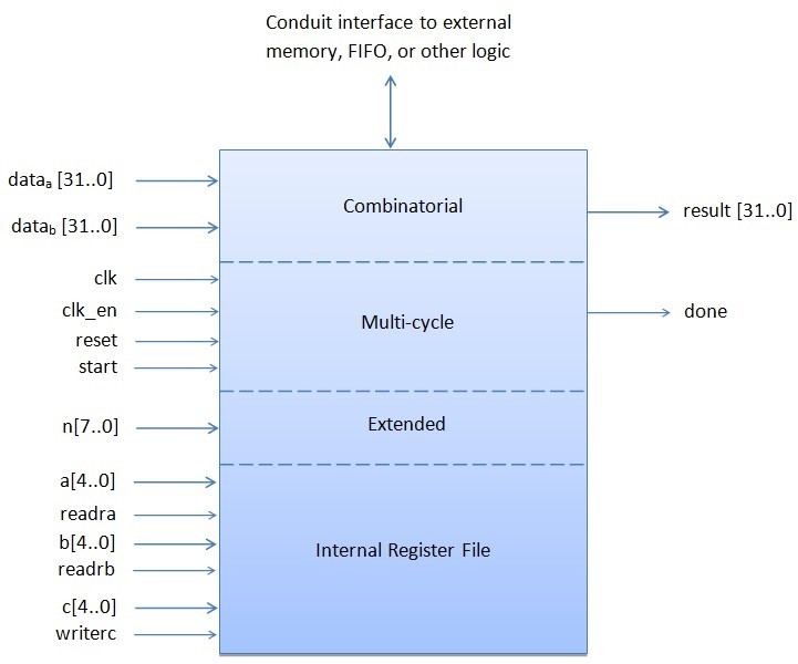
Table 2: FPH-2 operations implemented
Floating Point Hardware 2 custom instruction | |
Multi-Cycle Custom Instruction | Combinatorial Custom Instruction |
add multiply subtract divide square root convert | minimum maximum absolute compare negate |
Minimum, maximum, negate, absolute, and comparisons are all provided via the special instruction implementations. FPH-2 is preferred over FPH-1 legacy because it has a lower clock cycle count, better acceleration, and a smaller area. In addition, the FPH-2 component helps with FPH-1 procedures and rounding accuracy, which is not an IEEE 754-defined rounding mode [30]. The floating functions performed by each custom orders are listed in Table 2.
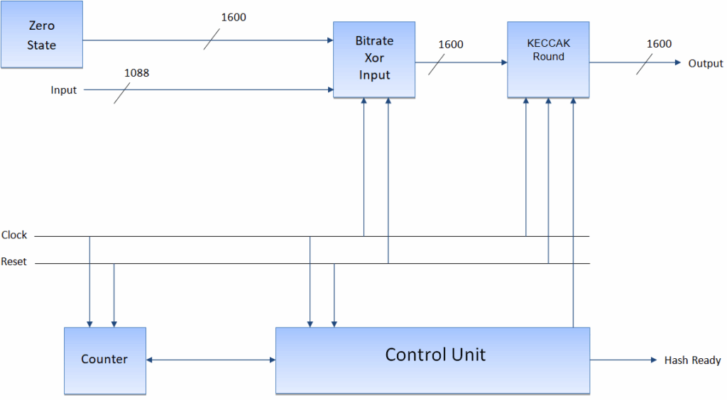
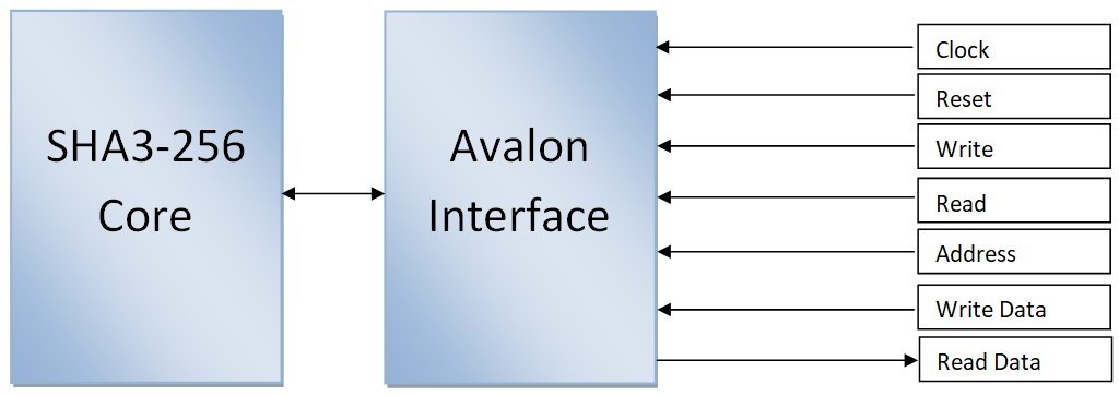
3.4. System Design of the SHA3-256 Core
FPH-2 is supported by the Nios II architecture. Low cycle count implementations are possible with the FPH-2 component. Addition, subtraction, square root integer to float conversion, multiplication, float to integer conversion, and division are the most common floating point custom in- structions. The SHA3-256 proposed system is depicted in Figure 3. The Xor Input bitrate, Zero State, Control Unit, Counter and Keccak Round are built into the structure. The initial zero status is retained in the zero status component of the first iteration of SHA-3.
While compile a multi-block message, the multiplexer is used to provide feedback. The Xor Input bitrate element combines the XOR bits of the bitrate state matrix with the bits of the Input block, which are the result of the infill procedure. The control, coordination and communication of the data flow within the design is the responsibility of the control unit. The Control Unit signal enables the meter. The Keccak RC is described in the following subsection.
3.5. The SHA-3 Pipelined Design
The SHA-3 has 24 modification phases, each of which is made up of five phases: θ, ρ, π, χ and ι, signified as theta, rho, pi, chi, and iota respectively. SHA-3 (Keccak) takes the state array per step and produces a newly updated state array after using the related state function. Figure 4 shows the Keccak Round’s two-staged pipelined design.
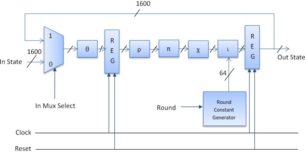
There is a 2-in-1 multiplexer for the round’s feedback at the start of the round. In each round, we use the pipelined approach to enter two registers. Between portions, the first register is located θ and ρ in order to separate the crucial path by nearly half. The second register is located just before the feedback unit at the end of the round. The clock and reset are the control signals of the two registers. The RC is put in the ι procedure produced by the RC generator and is shown in Table 3.
3.6. System Integration
The original grayscale image had a resolution of 256 × 256 pixels. The SDRAM memory stores the input block. The block is then fed into the SHA-3 core as input. The SHA-3 core’s output block is saved in SDRAM memory. VHDL was used to implement all of the components. Using a variety of test benches, we inspected each VHDL file to ensure its validity and usefulness. The ModelSim 10.6d simulator was used to run all of the tests on each VHDL file, with valid input data sheets given by NIST for the SHA-3 algorithm in [31].
In addition, we used ModelSim 10.6d to simulate the top module using legitimate input examples for the SHA-3 algorithm provided by NIST in [32]. We moved on to the design of the Nios II CPU after correctly verifying the simulation outcomes in ModelSim 10.6d.
Table 3: The RC Generator RCi in Iota function
RC0 | 0x0000000000000001 | RC12 | 0x000000008000808B |
RC1 | 0x0000000000008082 | RC13 | 0x800000000000008B |
RC2 | 0x800000000000808A | RC14 | 0x8000000000008089 |
RC3 | 0x8000000080008000 | RC15 | 0x8000000000008003 |
RC4 | 0x000000000000808B | RC16 | 0x8000000000008002 |
RC5 | 0x0000000080000001 | RC17 | 0x8000000000000080 |
RC6 | 0x8000000080008081 | RC18 | 0x000000000000800A |
RC7 | 0x8000000000008009 | RC19 | 0x800000008000000A |
RC8 | 0x000000000000008A | RC20 | 0x8000000080008081 |
RC9 | 0x0000000000000088 | RC21 | 0x8000000000008080 |
RC10 | 0x0000000080008009 | RC22 | 0x0000000080000001 |
RC11 | 0x000000008000000A | RC23 | 0x8000000080008008 |
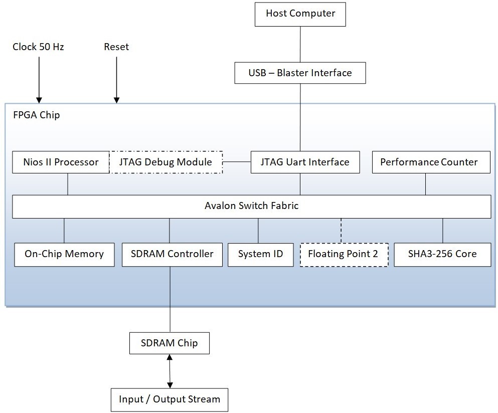
The designer platform was used to create the Nios II pro- cessor’s scheme. We utilised the Nios II fast soft-core, which has a high-performance speed and maximises the processor core’s fMAX performance. Clock, On-chip RAM, controller of SDRAM, a counter of performance, PLL, Peripheral ID System, JTAG-UART, and custom component SHA-3-256 are among the Nios II system’s implemented components. The operating memory for the Nios II CPU is on-chip RAM. As demonstrated in Figure 5, all information is sent from Nios II to the SHA-3 feature via the Avalon Switch Fabric.
Figure 6 displays the whole structure of our architecture that we built using the Nios II soft-core.
4. Experimental Results
The test were carried out using the Arria 10 GX FPGA. We designed a novel two-staged pipelined design with the FPH-2 component and a two-staged pipelined design.
4.1. Image and Histogram Analysis
Figure 7 (b) shows the histogram of the classical images (“Lena”, “Camera man” and “Pepper”) in Figure 7 (a). In the histogram, the horizontal axis denotes the gray level, and the vertical axis denotes the pixel number of each gray level. After being encrypted by the SHA3-256 (Keccak) algorithm, the histogram of the cipher-image is completely uniform and absolutely different from that of the plain-image as shown in Figure 7 (d).
4.2. Entropy Analysis
The entropy of a photograph is a statistical metric for de- termining how random a coded image is. It also describes the median information of an image origin. The entropy E(X) is calculated in (1), where X represents the test photo, xi symbolizes the cost in X, and Pr(xi) indicates the chance of X = xi.
$$E(X) = \sum_{i=1}^{n} \Pr(x_i) \log_2 \Pr(x_i)
\tag{1}$$
Table 4: The entropies of fragmented images and comparison
Images | This Work | Ref.[6] | Ref.[7] | Ref.[8] |
Boat | 7.9994 | 7.991 | 7.9993 | 7.991 |
Lena | 7.9990 | 7.990 | 7.9989 | – |
Cameraman | 7.9992 | – | 7.9991 | – |
Peppers | 7.9995 | – | 7.9994 | 7.991 |
Baboon | 7.9996 | 7.992 | 7.9995 | 7.992 |
The entropy of a large number of hashed photos was calculated. The results are presented in Table 4, which shows that the hashed image entropy’s are extremely near to 8. For a 256 gray-scale photo, the max entropy is log2(256) = 8. As a result, the suggested picture hashing approach has a high resistance against entropy attacks.
4.3. Correlation Analysis
Pixels should have a strong neighborhood correlation, which is one of the most important properties of an image. For the design to be considered secure and effective, there must be no correlation between pixels in an encrypted image. The correlation coefficient is given by in (2), where xi and yi is a pair of neighboring pixels that are horizontally, vertically, and diagonally adjacent, M signifies the total number of neighboring pixel pairs.
$$r_{xy} = \frac{\sum_{i=1}^{M} \left(x_i – \frac{1}{M} \sum_{j=1}^{M} x_j \right)\left(y_i – \frac{1}{M} \sum_{j=1}^{M} y_j \right)}{\sqrt{\sum_{i=1}^{M} \left(x_i – \frac{1}{M} \sum_{j=1}^{M} x_j \right)^2} \sqrt{\sum_{i=1}^{M} \left(y_i – \frac{1}{M} \sum_{j=1}^{M} y_j \right)^2}}\tag{2}$$
Table 5 shows the correlation coefficients in the three orientations, demonstrating that the encrypted image cor- relation coefficients are very close to 0. As a result, the suggested model is resistant to statistical attacks.
Table 5: Correlations coefficients of encrypted images
Image | Direction | Correlation |
Lena | Horizontal | 0.001214 |
Vertical | 0.006210 | |
Diagonal | 0.003216 | |
Camera man | Horizontal | 0.001368 |
Vertical | 0.007410 | |
Diagonal | 0.004126 | |
Peppers | Horizontal | 0.001424 |
Vertical | 0.007128 | |
Diagonal | 0.005210 |
4.4. NPCR and UACI Metrics Analysis
We use the Number of Pixel Change Rates (NPCR) and Unified Average Changing Intensity (UACI) to calculate the result of switching one pixel in both plain and hashed photos. [33]. The NPCR measures the number of individual pixels between the two images, and the UACI measures the average intensity. The NPCR is computed using (3), where D represents the bipolarity array with comparable size as the prototype image and hashes image, M × N define the size of the picture.
$$\text{NPCR} = \sum_{i=1}^{M} \sum_{j=1}^{N} D(i,j) \times \frac{100\%}{M \times N}\tag{3}$$
The UACI calculated using (4), where C1 denotes the original image, C2 is the hashed picture and M × N define the size of the picture in pixels.
$$\text{UACI} = \left[ \sum_{i=1}^{M} \sum_{j=1}^{N} \frac{|C_1(i,j) – C_2(i,j)|}{255} \right] \times \frac{100\%}{M \times N}\tag{4}$$
The findings of the NPCR and the UACI are shown in Table 6. The high values of the NPCR and UACI measure- ments imply that hashing is more secure and more resistant to differential assaults.
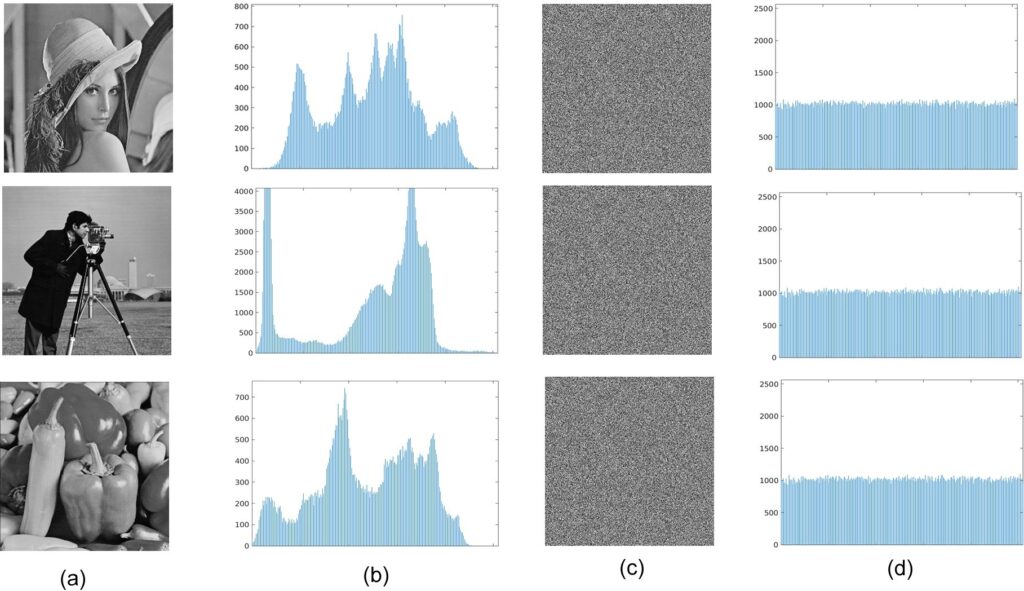
Table 6: The NPCR and the UACI results and comparison
Images | This Work | Ref. [6] | Ref. [7] | Ref. [8] | ||||
NPCR | UACI | NPCR | UACI | NPCR | UACI | NPCR | UACI | |
Boat | 99.644 | 33.652 | 99.629 | 33.529 | 99.6420 | 33.6463 | – | – |
Lena | 99.692 | 33.688 | 99.554 | 33.392 | 99.6886 | 33.6818 | 99.603 | 33.432 |
Cameraman | 99.660 | 33.662 | 99.598 | 33.534 | 99.6543 | 33.6592 | 99.641 | 33.498 |
Peppers | 99.634 | 33.640 | – | – | 99.6321 | 33.6326 | – | – |
Baboon | 99.662 | 33.664 | 99.615 | 33.402 | 99.6563 | 33.6531 | 99.600 | 33.428 |
4.5. Throughput and Efficiency Metrics
The throughput (TH) is computed using (5). In the (5), Number of bits is the bitrate size r, frequency is the maximum frequency reported by the tool and Number of clock cycles denote the latency of the circuit. Clock cycles represent the number of resumption needed of the five functions θ, ρ, π, χ and ι to generate the hash value.
$$TH = \frac{\textit{Number of bits} \times \textit{frequency}}{\textit{Number of clock cycles}}\tag{5}$$
The efficiency (EF) is computed by using (6).
$$EF = \frac{TH}{\textit{Area}}\tag{6}$$
The findings of our two designs for the SHA3-256 (Kec- cak) algorithm are shown in Table 7. The number of clock cycles of the five functions in a two-staged pipelined design is 18, while the number of clock cycles in a two-staged pipelined design with the component FPH-2 is 14.
Since the number of clock cycles is reduced and the maximum clock frequency increases, the proposed design of a two-staged pipelined architecture with FPH-2 provides the highest efficiency and throughput.
Table 7: The results for Efficiency and Throughput of our two designs
Design | Area (Slices) | Frequency (MHz) | Throughput (Gbps) (r = 1088) | Efficiency (Mbps/Slices) (r = 1088) |
Proposed architecture with two-staged pipeline | 2682 | 432 | 25.507 | 9.51 |
Proposed architecture with two-staged pipeline and FPH-2 | 2764 | 472 | 36.681 | 13.27 |
Table 8 presents the comparison with other similar ar- chitectures, taking into account their best implementation in terms of the criteria of throughput and efficiency for the SHA3-256 (Keccak) algorithm. When using the component FPH-2 to implement the proposed design, the area was raised by 10.30% (slices), but the maximum clock improved by 10.92% (frequency) and increased by 12.85% the number of clock cycles, resulting in a 14.38% increase in throughput and a 13.95% increase inefficiency.
Researchers in the works [9, 11, 12, 13, 20, 21, 22] show a smaller area compared to our implementations, but the frequency they achieve is lower than our experimental ap- plications. Also, in the work [15] there is a higher frequency than the one we achieved, but they show a large increase in the area. Finally, in the works [7, 14, 18] the researchers
Table 8: Throughput – Efficiency results and comparison for the SHA-3 algorithm
Work | FPGA Device | Frequency (MHz) | Area (Slices) | Throughput (Gbps) (r = 1088) | Efficiency (Mbps/Slices) (r = 1088) |
Kitsos P. et al. (2010) [14] | – | 215 | 4745 | 11.9 | 2.50 |
Akin A. et al. (2010) [15] | Virtex-4 | 509 | 4356 | 22.33 | 5.13 |
Kaps J. P. et al. (2012) [21] | Virtex-6 | 299 | 106 | 0.136 | 1.28 |
Provelengios G. et al. (2012) [20] | Virtex-5 | 285 | 2573 | 5.70 | 2.21 |
Gaj K. et al. (2010) [12] | Virtex-6 | 282.7 | 1272 | 12.817 | 10.08 |
Jararweh Y. et al. (2012) [11] | Virtex-5 | 271 | 1414 | 12.28 | 8.68 |
Sideris A.et al. (2022) [7] | Arria 10 GX | 458 | 2984 | 35.593 | 11.92 |
Gholipour A. et al. (2012) [18] | Altera Stratix III | 212.49 | 5633 | 13.59 | 2.41 |
Baldwin B. et al. (2010) [13] | Virtex-5 | 189 | 1117 | 6.263 | 3.17 |
Kobayashi K. et al. (2010) [22] | Virtex-5 | 205 | 1433 | 8.40 | 5.86 |
Homsirikamol E. et al. (2011) [10] | Virtex-6 | – | 1446 | 16.236 | 11.23 |
Jungk B. (2011) [9] | Virtex-6 | 197 | 397 | 1.071 | 2.69 |
Proposed design with FPH-2 | Arria 10 GX | 472 | 2764 | 36.681 | 13.27 |
show a larger area and smaller frequency than we achieved with our architectures. In our architectures, the primary purpose was not to use an excessive growth of the cost of the area (Slices) so that the throughput (Gbps) and efficiency (Mbps/Slices) are not burdened.
5. Conclusions and Future Work
The optimal performance of hashing images with a size of 256 × 256 pixels using the SHA-3 algorithm with the Nios II/f (fast) soft-core processor in the FPGA Intel Arria 10 GX is presented in this study.
We choose the SHA-3 algorithm, which has a 256-bit output length, because it provides the best security and performance. Our testing using the proposed two-staged pipelined design and the bespoke FPH-2 component re- vealed that the SHA-3 algorithm had a 14.38% percent improvement in throughput and a 13.95% percent gain in- efficiency. At the same time, we increased the minimum area by 10.30% (slices), the max clock signal by 10.92% (fre- quency), and by 12.85% the number of clock cycles. The suggested approach combines speed, performance, and se- curity to produce the optimum solution for hashing images with a dimension of 256 × 256 pixels.
In the future, we’ll experiment with picture hashing using Tree Hashing and a simpler design with fewer rounds (12 instead of the 24 in SHA-3).
Conflict of Interest The authors declare no conflict of interest.
- S. Agarwal, “Secure image transmission using fractal and 2d- chaotic map”, Journal of Imaging, vol. 4, no. 1, p. 17, 2018, doi: 10.3390/jimaging4010017.
- A. Girdhar, H. Kapur, V. Kumar, “A novel grayscale image encryption and image blocks”, Applied Physics
- X. Kang, R. Tao, “Color image encryption using pixel scrambling operator and reality-preserving mpfrht”, IEEE Transactions on Circuits and Systems for Video Technology, vol. 29, no. 7, pp. 1919–1932, 2018, doi:10.1109/TCSVT.2018.2859253.
- A. Swaminathan, Y. Mao, M. Wu, “Robust and secure image hashing”, IEEE Transactions on Information Forensics and security, vol. 1, no. 2, pp. 215–230, 2006, doi:10.1109/TIFS.2006.873601.
- V. Monga, A. Banerjee, B. L. Evans, “A clustering based approach to perceptual image hashing”, IEEE Transactions on Information Forensics and Security, vol. 1, no. 1, pp. 68–79, 2006, doi:10.1109/TIFS.2005.863502.
- G. Ye, H. Zhao, H. Chai, “Chaotic image encryption algorithm us- ing wave-line permutation and block diffusion”, Nonlinear Dynamics, vol. 83, no. 4, pp. 2067–2077, 2016, doi:10.1007/s11071-015-2465-7.
- A. Sideris, T. Sanida, D. Tsiktsiris, M. Dasygenis, “Image hashing based on sha-3 implemented on fpga”, “Recent Advances in Manu- facturing Modelling and Optimization”, pp. 521–530, Springer, 2022, doi:10.1007/978-981-16-9952-8_44.
- G. Ye, X. Huang, “A secure image encryption algorithm based on chaotic maps and SHA-3”, Security and Communication Networks, vol. 9, no. 13, pp. 2015–2023, 2016, doi:10.1002/sec.1458.
- B. Jungk, J. Apfelbeck, “Area-efficient fpga implementations of the sha-3 finalists”, “2011 International Conference on Reconfig- urable Computing and FPGAs”, pp. 235–241, IEEE, 2011, doi: 10.1109/ReConFig.2011.16.
- E. Homsirikamol, M. Rogawski, K. Gaj, “Comparing hardware per- formance of round 3 sha-3 candidates using multiple hardware architectures in xilinx and altera fpgas”, “Ecrypt II Hash Workshop”, vol. 2011, pp. 1–15, 2011, doi:10.1001/ICT-2007-216676.
- Y. Jararweh, H. Tawalbeh, A. Moh’d, et al., “Hardware performance evaluation of sha-3 candidate algorithms”, Journal of Information Security, 2012, doi:10.4236/jis.2012.32008.
- K. Gaj, E. Homsirikamol, M. Rogawski, “Fair and comprehensive methodology for comparing hardware performance of fourteen round two sha-3 candidates using FPGAs”, “International Workshop on Cryptographic Hardware and Embedded Systems”, pp. 264–278, Springer, 2010, doi:10.1007/978-3-642-15031-9_18.
- B. Baldwin, A. Byrne, L. Lu, M. Hamilton, N. Hanley, M. O’Neill, W. P. Marnane, “FPGA implementations of the round two sha-3 candidates”, in Field Programmable Logic and ons”, pp. 400–407, IEEE, 2010, doi:10.1109/FPL.2010.84.
- P. Kitsos, N. Sklavos, “On the hardware implementation efficiency of sha-3 candidates”, “2010 17th IEEE International Conference on electronics, Circuits and Syst 3, IEEE, 2010, doi: 2010.5724743.
- P. Kitsos, N. Sklavos, “On the hardware implementation efficiency of sha-3 candidates”, “2010 17th IEEE International Conference on Electronics, Circuits and Systems”, pp. 1240–1243, IEEE, 2010, doi: 10.1109/ICECS.2010.5724743.
- A. Akin, A. Aysu, O. C. Ulusel, E. Savaş, “Efficient hardware imple- mentations of high throughput sha-3 candidates keccak, luffa and blue midnight wish for single-and multi-message hashing”, “Proceedings of the 3rd International Conference on Security of Information and Networks”, pp. 168–177, 2010, doi:10.1145/1854099.1854135.
- I. San, N. At, “Compact keccak hardware architecture for data integrity and authentication on fpgas”, Information Security Jour- nal: A Global Perspective, vol. 21, no. 5, pp. 231–242, 2012, doi: 10.1080/19393555.2012.660678.
- A. Sideris, T. Sanida, M. Dasygenis, “High throughput pipelined implementation of the sha-3 cryptoprocessor”, “2020 32nd Interna- tional Conference on Microelectronics (ICM)”, pp. 1–4, IEEE, 2020, doi:10.1109/ICM50269.2020.9331803.
- A. Gholipour, S. Mirzakuchaki, “High-speed implementation of the keccak hash function on fpga”, International Journal of Ad- vanced Computer Science, vol. 2, no. 8, pp. 303–307, 2012, doi: 10.1142/S0218126616500262.
- A. Sideris, T. Sanida, M. Dasygenis, “High throughput implementation of the keccak hash function using the nios-ii processor”, Technologies, vol. 8, no. 1, p. 15, 2020, doi:10.3390/technologies8010015.
- G. Provelengios, P. Kitsos, N. Sklavos, C. Koulamas, “Fpga-based design approaches of keccak hash function”, “2012 15th Euromi- cro Conference on Digital System Design”, pp. 648–653, IEEE, 2012, doi:10.1109/DSD.2012.63.
- J.-P. Kaps, P. Yalla, K. K. Surapathi, B. Habib, S. Vadlamudi, S. Gu- rung, “Lightweight implementations of sha-3 finalists on fpgas”, “The Third SHA-3 Candidate Conference”, pp. 1–17, 2012, doi: 10.1007/978-3-642-25578-6_20.
- K. Kobayashi, J. Ikegami, M. Knežević, E. X. Guo, S. Matsuo, S. Huang, L. Nazhandali, Ü. Kocabaş, J. Fan, A. Satoh, et al., “Prototyping plat- form for performance evaluation of sha-3 candidates”, “2010 IEEE International Symposium on Hardware-Oriented Security and Trust (HOST)”, pp. 60–63, IEEE, 2010, doi:10.1109/HST.2010.5513111.
- F. Kahri, H. Mestiri, B. Bouallegue, M. Machhout, “High speed fpga implementation of cryptographic keccak hash function crypto- processor”, Journal of Circuits, Systems and Computers, vol. 25, no. 04, p. 1650026, 2016, doi:10.1142/S0218126616500262.
- G. S. Athanasiou, G.-P. Makkas, G. Theodoridis, “High throughput pipelined fpga implementation of the new sha-3 cryptographic hash algorithm”, “2014 6th International Symposium on Communications, Control and Signal Processing (ISCCSP)”, pp. 538–541, IEEE, 2014, doi:10.1109/ISCCSP.2014.6877931.
- L. Ioannou, H. E. Michail, A. G. Voyiatzis, “High performance pipelined fpga implementation of the sha-3 hash algorithm”, “2015 4th Mediterranean Conference on Embedded Computing (MECO)”, pp. 68–71, IEEE, 2015, doi:10.1109/MECO.2015.7181868.
- Intel®FPGA, “Classic processor reference guide”, online https://www.intel.com/content/dam/www/programmable/ us/en/pdfs/literature/hb/nios2/n2cpu_nii5v1.pdf , (accessed on 12 December 2021).
- A. Sideris, T. Sanida, M. Dasygenis, “Hardware acceleration of sha-256 algorithm using nios-ii processor”, “2019 8th International Conference Technologies (MOCAST)”, pp.109/MOCAST.2019.8741638.
- A. Sideris, T. Sanida, M. Dasygenis, “Hardware acceleration of the aes algorithm using nios-ii processor”, “2019 Panhellenic Conference on Electronics & Telecommunications (PACET)”, pp. 1–5, IEEE, 2019, doi:10.1109/PACET48583.2019.8956285.
- Intel®FPGA, “Nios II custom instruction user guide”, on- line https://www.intel.com/content/www/us/en/programmable/ documentation/cru1439932898327.html, (accessed on 20 December 2021).
- NIST, “Cryptographic standards and guide- lines”, online https://csrc.nist.gov/Projects/ Cryptographic-Standards-and-Guidelines, (accessed on 10 December 2021).
- CSDITL, “Example values – cryptographic standards and guidelines”, online https://csrc.nist.gov/projects/ cryptographic-standards-and-guidelines/example-values, (accessed on 19 December 2021).
- Y. Wu, J. P. Noonan, S. Agaian, et al., “NPCR and UACI randomness tests for image encryption”, Cyber journals: multidisciplinary journals in Telecommunications 2011, doi:10.1001/JSAT.2011.863-502-2.