An Advanced Load-Line Analysis Software for use in the Design and Simulation of Microwave Low-Distortion, High-Efficiency and High-Power GaN HEMT Amplifiers
(This article belongs to the Section Electronic Engineering (EEE))
Export Citations
Cite
Itoh, Y. , Kaho, T. and Matsunaga, K. (2023). An Advanced Load-Line Analysis Software for use in the Design and Simulation of Microwave Low-Distortion, High-Efficiency and High-Power GaN HEMT Amplifiers. Journal of Engineering Research and Sciences, 2(4), 14–21. https://doi.org/10.55708/js0204002
Yasushi Itoh, Takana Kaho and Koji Matsunaga. "An Advanced Load-Line Analysis Software for use in the Design and Simulation of Microwave Low-Distortion, High-Efficiency and High-Power GaN HEMT Amplifiers." Journal of Engineering Research and Sciences 2, no. 4 (April 2023): 14–21. https://doi.org/10.55708/js0204002
Y. Itoh, T. Kaho and K. Matsunaga, "An Advanced Load-Line Analysis Software for use in the Design and Simulation of Microwave Low-Distortion, High-Efficiency and High-Power GaN HEMT Amplifiers," Journal of Engineering Research and Sciences, vol. 2, no. 4, pp. 14–21, Apr. 2023, doi: 10.55708/js0204002.
An advanced load-line analysis software is devised for nonlinear circuit design and simulation of microwave low-distortion, high-efficiency and high-power GaN HEMT amplifiers. A single software package can incorporate DC, small- and large-signal performances of GaN HEMT devices, and then analyze nonlinear performance of amplitude-to-amplitude (AM-AM) and amplitude-to-phase (AM-PM) modulations, and finally evaluate intermodulation distortion (IMD) and error vector measurement (EVM). High speed and high accurate simulation become available with the use of behavioral modeling for representing nonlinear performance of GaN HEMT devices. In addition, the software employs a time-domain analysis using time-varying electrical waveform and thus give clear and deep insight into the nonlinear behavior of GaN HEMT devices as well as the nonlinear circuit design technique of low-distortion and high-efficiency amplifiers. In comparison with the harmonic-balance (HB) method, comparable performances have been successfully achieved for an L-band 10W GaN HEMT amplifier.
1. Introduction
In recent years, low-distortion and high-efficiency of microwave high-power amplifiers represent one of the most crucial design issues in order to meet the stringent requirements of reduced cost and excellent thermal treatment of the modern wireless transmitting systems. As a starting point of power amplifier (PA) designs, the Cripps load-line theory [1] is widely used to know available output power and efficiency as well as load conditions. The Cripps load-line theory, however, has adopted the simplified device description and thus strong nonlinearity including hard saturation, large leakage current and low-frequency dispersion effects of GaN HEMT devices cannot be accurately described [2-3]. Therefore, the PA designs utilize the active and/or passive load-pull measurements as a following step to know the optimum load impedances under the actual operating conditions [4]. The load-pull measurements are, however, limited by frequency, power, impedance range, number of harmonics and stability [5]. Therefore, most of the PA designs move to the nonlinear circuit simulations using harmonic-balance method [6]. The harmonic-balance method requires the accurate nonlinear device models. Indeed, the load-pull measurement and the harmonic-balance simulation are actually a powerful tool for PA designs but only a few information on the PA designs related to low-distortion and high-efficiency can be derived. On the other hand, the load-line theory is based on time-domain waveform analysis and thus provides much useful information on load and bias conditions for low-distortion and high-efficiency.
The author has presented the nonlinear load-line analysis method to demonstrate AM-AM and AM-PM characteristics of GaAs MESFET devices in 1995 [7] and in 2001 [8]. The method, however, cannot deal with strong nonlinearity such as hard saturation and large leakage currents. Moreover, the method is based on the measured data and thus time-consuming and inaccurate simulations were crucial design issues. In order to address these design issues, behavioral modeling is utilized to represent nonlinearity of GaN HEMT devices. Moreover, the calculated AM-AM and AM-PM characteristics are represented by behavioral modeling. It makes available the 2-tone power series and envelope analyses including IP and IMD as well as EVM [9] evaluation of the modern wireless transmitting systems with high speed and high accuracy. The load-line analysis method presented here can be performed to run software written by MATLAB R2021b [10]. This is the first nonlinear load-line analysis software package ever reported. An L-band 10W GaN HEMT amplifier has been designed by using this software and compared with the harmonic-balance method [6] to make sure the validity of the software.
2. Advanced Techniques in Load-Line Analysis
2.1. Time-Varying Electrical Waveform Analysis
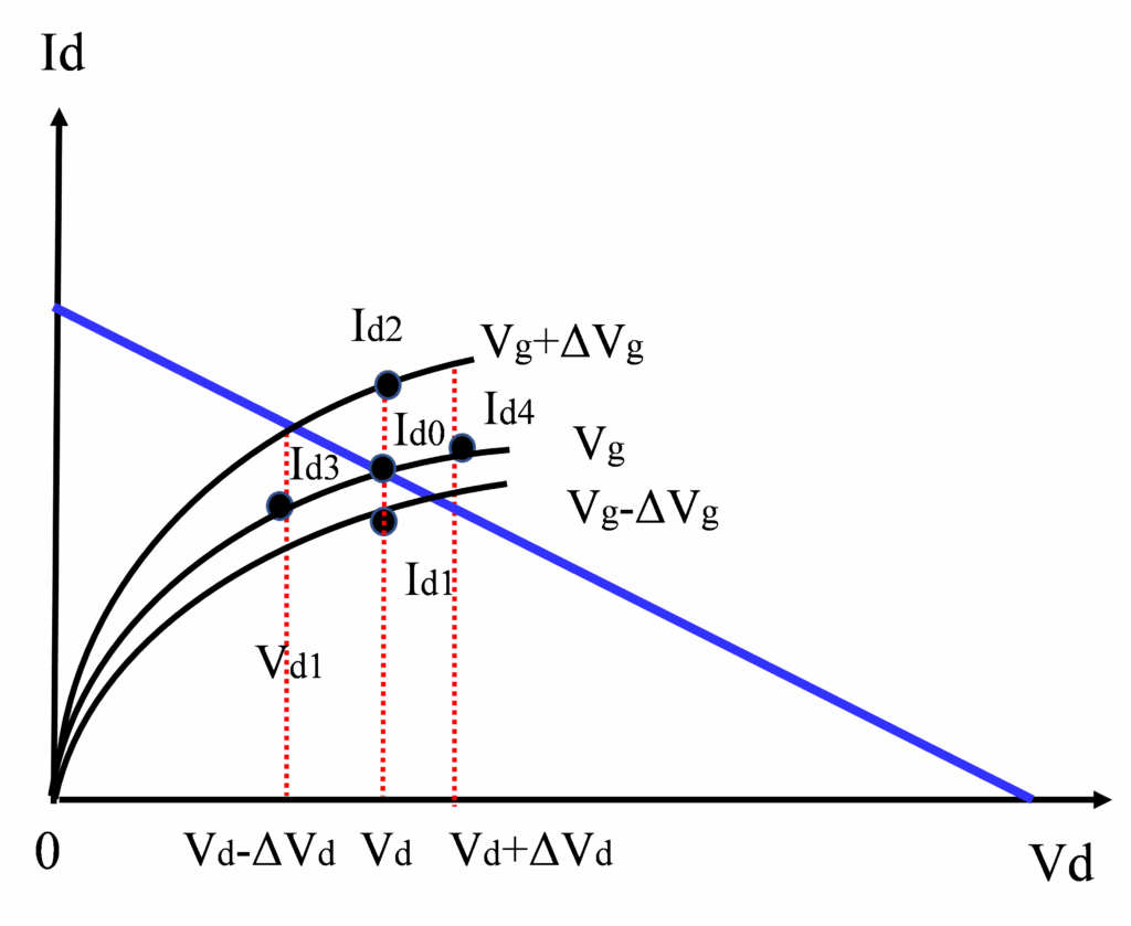
Principles of the load-line analysis is shown in Figure 1 [7]. Drain current Id(t) and drain voltage Vd(t) swing on the load-line having a resistive slope of -gl within the area surrounded by Vk (Knee voltage), Vbr (breakdown voltage), Vbr+Vp (Vp is a pinchoff voltage) and zero. As a magnitude of Id(t), denoted as A(J), increases with input power, the upper or the lower-half of Id(t) is clipped by Idss or zero. That is, DC component of Id(t) expanded by Fourier series increases or decreases. It means that the initial bias point a (Vdo, Ido) moves to a different bias point. For example, under class-AB or B operation, the lower half of Id(t) is clipped first. DC component increases and the bias point moves upward in conjunction with the load-line. Next the upper-half of Id(t) is clipped. DC component decreases and the bias point moves downward in conjunction with the load-line. This procedure is repeated until the bias point converges to some quiescent bias point b (Vdo, Idav).
Figure 1: Principles of the load-line analysis. Drain current Id(t) and drain voltage Vd(t) swing on the load-line having a resistive slope of -gl within the area surrounded by Vk (Knee voltage), Vbr (breakdown voltage), Vbr+Vp (Vp is a pinchoff voltage) and zero. Point a is an initial bias condition (Vdo, Ido). Point b is a final bias condition (Vdo, Idav).
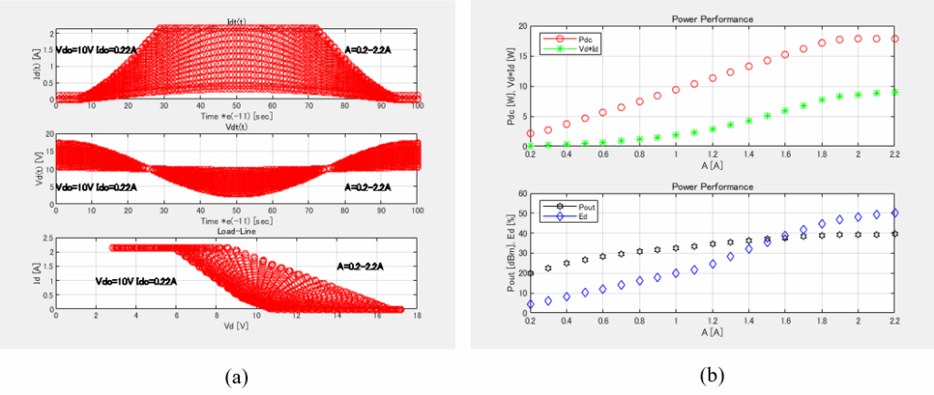
Id(t), Vd(t), a dynamic load-line are calculated by this load-line analysis software for GaN HEMT devices with Vk of 2V, Vbr of 100V, Vp of -2V and Idss of 2.14A, which is shown in Figure 2(a). As A(J) increases from 0.2 to 2.2A, Id(t) and Vd(t) also increase and the bias point moves upward from the initial point (10V, 0.214A) in conjunction with the load-line. The slope of -gl can be varied as a dynamic load-line but keep constant in this case. Output power (Pout), drain efficiency (hd), DC consumption power (Pdc) and Vd x Id can be calculated for a variation of A(J) and plotted in Figure 2(b). As A(J) increases, Pout goes up to 10W and hd also increases.
2.2. Large-Signal GaN HEMT Model Used in the Analysis
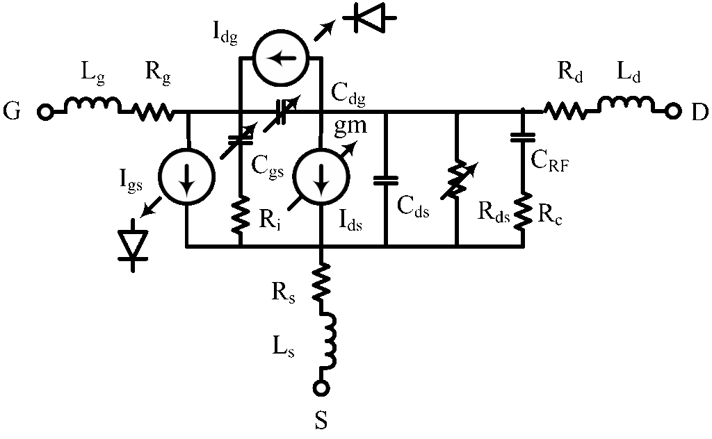
A large-signal GaN HEMT model is employed in the analysis, which is shown in Figure 3. Nonlinear circuit elements are transconductance (gm), drain-to-source resistance (Rds), gate-to-source capacitance (Cgs) and gate-to-drain capacitance (Cdg), which are obtained from I-V curves as a function of the gate voltage (Vg) and the drain voltage (Vd). A forward gate current (Igs) and a backward gate leakage current (Idg) are also included in the analysis for hard saturation and large leakage conditions. The nonlinear circuit elements (gm, Rds, Cgs, Cdg) and the gate current (Ids and Idg) are basically represented by behavioral modeling [11].
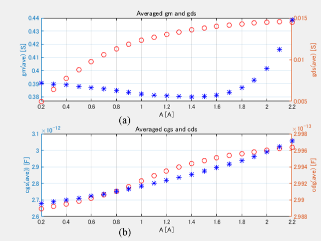
Nonlinear circuit elements of gm, Rds, Cgs and Cdg are obtained from I-V curves as a function of Vg and Vd, which is shown in Figure 4. Since Id(t) moves on the load-line with A(J), gm and gds (=1/Rds) defined by (1) and (2) varies with A(J). Under large-signal operation, therefore, gm and gds are represented as an averaged value for one period, which are given as gmave and gdsave by (3) and (4) [8]. Id (Vg, Vd) is represented by behavioral modeling in place of the measured data for high speed and high accurate calculation. The Curtice Cubic Model [12] is used here.
$$gm = \lim_{\Delta V_g \to 0} \frac{I_d(V_g + \Delta V_g, I_d) – I_d(V_g, I_d)}{\Delta V_g}\tag{1}$$
$$g_{ds} = \lim_{\Delta V_d \to 0} \frac{I_d(V_g, V_d + \Delta V_d) – I_d(V_g, V_d)}{\Delta V_d}\tag{2}$$
$$gm_{av} = \frac{1}{T} \int_0^T gm(t)dt = \frac{1}{N} \sum_{n=1}^{N} gm(n)\tag{3}$$
$$gds_{av} = \frac{1}{T} \int_0^T g_{ds}(t)dt = \frac{1}{N} \sum_{n=1}^{N} gds(n)\tag{4}$$
Cgs and Cdg defined by (5) and (6) also varies with A(J) on the load-line. Under large-signal operation, therefore, Cgs and Cdg are represented as an averaged value for one period, which are given as Cgsave and Cdgave by (7) and (8) [9-10]. In (5) and (6), Cgs and Cds utilize the Statz model [13].
$$C_{gs} = C_{gs1} + \frac{C_{gs0}}{\left(1 – \frac{V_g}{V_{bi}}\right)^m} + C_{gs2} V_d\tag{5}$$
$$C_{dg} = C_{dg1} + \frac{C_{dg0}}{\left(1 – \frac{V_d – V_g}{V_{bi}}\right)^n}\tag{6}$$
$$C_{gsav} = \frac{1}{N} \sum_{l=1}^{N} C_{gs}(l)\tag{7}$$
$$C_{dgav} = \frac{1}{N} \sum_{l=1}^{N} C_{dg}(l)\tag{8}$$
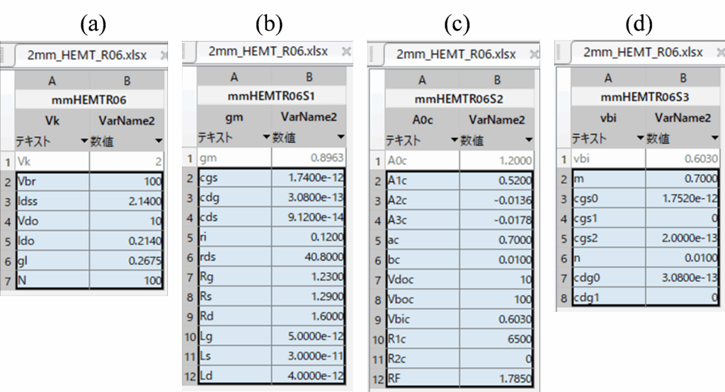
DC, small-signal, large-signal circuit elements as well as nonlinear capacitances consisting of Figure 3 can be read from Microsoft Excel sheet, which are shown in Tables 1(a), 1(b), 1(c) and 1(d), respectively. With the use of these data, gmave, gdsave Cgsave and Cdgave are calculated and plotted in Figure 5. It is clearly shown that nonlinear elements are drastically change with A(J).
Table 1: DC, small-signal, large-signal circuit elements as well as nonlinear capacitances consisting of Figure 3
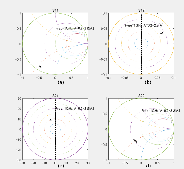
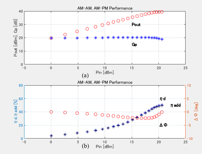
Since gmave, gdsave, Cgsave and Cdgave are obtained for each A(J), S-parameters of Figure 3 can be calculated, which is shown in Figure 6. A calculation was done for A(J) from 0.2 to 2.2A at 1GHz. Amid these parameters, S22 changes remarkably. A variation of Mag(S21) and Ang(S21) leads to AM-AM and AM-PM performances. In conjunction with the data in Figure 2(b), the output power (Pout), power gain (Gp), drain efficiency (hd), power-added efficiency (hadd) and insertion phase variation (Df) are calculated and plotted in Figure 7.
2.3. Behavioral Modeling
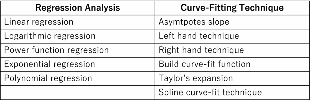
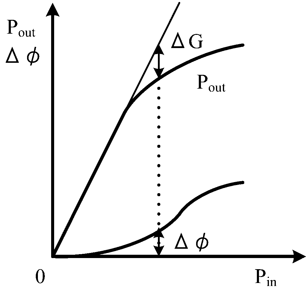
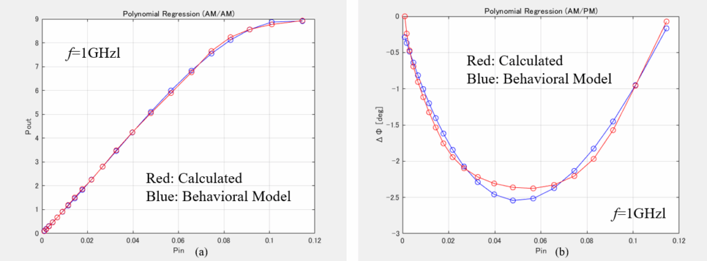
Once AM-AM and AM-PM performance are known, the distortion analyses including 2-tone power series analysis, 2-tone envelope analysis and EVM evaluation become available. Before the distortion analysis, AM-AM and AM-PM performances have to be represented by behavioral modeling for high speed and high accurate calculation. Behavioral modeling is listed in Table 2 [11]. The traditional distortion analysis of microwave power amplifiers deals with polynomial regression such as power series or Volterra series [1] because harmonic contents are easily handled. Thus, polynomial regression is employed here as behavioral modeling for representing AM-AM (Pout vs Pin) and AM-PM (Df vs Pin) performances shown in Figure 8.
Table 2: List of behavioral modeling: Behavioral modeling includes regression analysis and curve-fitting technique
Based on the AM-AM (Pout vs Pin) and AM-PM (Df vs Pin) performances of Figure 7, the 3rd polynomial equations are calculated, which are shown in (9) and (10). Pin and Pout are denoted as antilog value. Df is given as degree.
$$P_{out} = a_3 P_{in}^3 + a_2 P_{in}^2 + a_1 P_{in} + a_0$$
$$a_3 = -5.8643\text{E}3,$$
$$a_2 = 0.5233\text{E}3,$$
$$a_1 = 0.0946\text{E}3,$$
$$a_0 = 0 \tag{9}$$
$$\Delta \Phi = a_3 P_{in}^3 + a_2 P_{in}^2 + a_1 P_{in} + a_0$$
$$a_3 = -3.1400\text{E}3,$$
$$a_2 = 1.2512\text{E}3,$$
$$a_1 = -0.1019\text{E}3,$$
$$a_0 = -0.0002 \tag{10}$$
The calculated AM-AM and AM-PM performances shown in Figure 7 are also demonstrated in Figure 9 in conjunction with behavioral modeling. A good agreement has been achieved between the calculated and modeled data.
2.4. Distortion Analysis (2-tone Analysis)
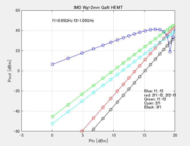
This load-line analysis software prepares two types of 2-tone analyses: 2-tone power series analysis for weak nonlinearity and 2-tone envelope analysis for strong nonlinearity [1]. For example, in the 3rd-order 2-tone power series analysis, 2-tone signal described in (11) and (12) is inserted into (9). Then the 2nd-degree term of (9) produces the 2nd-order product at 2w1, 2w2, w1+w2. The 3rd-degree term provides the 1st– and 3rd-order products at w1, w2, 3w1, 3w2, 2w1-w2, 2w2-w1. The 1st-, 2nd– and 3rd -order products are calculated and plotted as Pin-Pout in Figure 10. IIP3 can be easily obtained from the intersection point of an extended linear part of w1 and an extended linear part of w3.
$$P_{in} = v_1 \cos \omega_1 t + v_2 \cos \omega_2 t \tag{11}$$
$$v_1 = v_2 = v \tag{12}$$
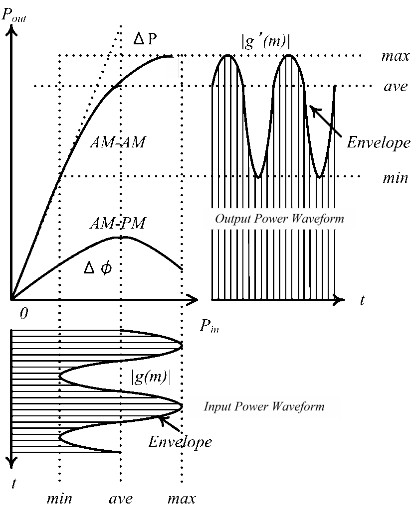
The 2-tone envelope analysis is shown in Figure 11 [1]. An envelope of the input 2-tone signal is modulated by a difference frequency of w1-w2 (w1> w2). The amplified output signal is distorted in both magnitude and phase through AM-AM and AM-PM performances of PAs, which produces a serious intermodulation distortion. Input and output signals are given by (13) and (14). The input time-domain signal g(m) can be transformed from the frequency-domain signal G(k) by the inverse Fourier transformation as (15). The input signal is amplified and then the time-domain output signal g’(m) is given by (16). Finally, the frequency-domain output signal G’(k) is transformed by Fourier transformation as (17).
$$V_i(t) = \text{Re}|\rho \cdot \exp(j\omega t)| \tag{13}$$
$$V_o(t) = \text{Re}|A(|\rho|) \cdot \exp(j\omega t + j\theta(|\rho|))| \tag{14}$$
$$g(m) = \sum_{k=0}^{N-1} G(k) \exp\left(\frac{i2\pi mk}{N}\right) \tag{15}$$
$$g'(m) = |A(g(m))| \cdot \exp(j\theta(g(m)))| \tag{16}$$
$$G'(n) = \frac{1}{N} \sum_{k=0}^{N-1} g'(k) \exp\left(-\frac{i2\pi nk}{N}\right) \tag{17}$$
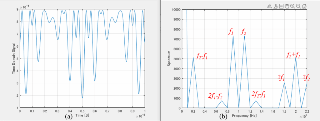
Time- and frequency-domain output signals are calculated with the use of 2-tone envelope analysis shown in Figure 11 and behavioral modeling of Figure 9 for 2-tone signal (f1=0.9GHz, f2=1.1GHz, v=0.02V) in (11) and (12), which are displayed in Figure 12. Figure 12(a) shows a time-domain output signal and Figure 12(b) displays a frequency-domain output signal (spectrum). IMD3 signals (2f1– f2 and 2f2– f1) appear adjacent to carrier signals (f1 and f2). In addition, a difference signal (f2– f1), a sum signal (f1+ f2), 2nd-harmonic signals (2f1 and 2f2) are also clearly shown. Due to the maximum limit of memory size of the computer, the resolution of spectrum becomes poor.
2.5. EVM Evaluation
Error vector magnitude (EVM) evaluation can provide a great deal of insight into the performances of digital communications transmitters and receivers [14]. The error vector is defined as a vector difference at a given time between the ideal reference signal and the measured signal, which is shown in Figure 13. AM-AM performance having DG and AM-PM performance having Df in Figure 13(a) produce a serious vector error in Figure 13(b).

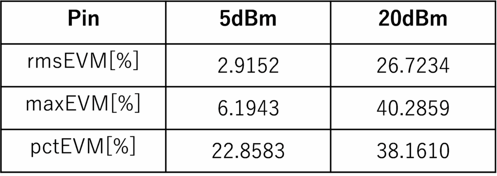
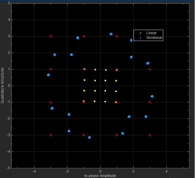
Now EVM is evaluated for GaN HEMT amplifiers having AM-AM and AM-PM performance shown in Figures 7, 9 and 13(a). EVM can be obtained by using MATLAB Simulink of EVM and MER measurement [15]. The explore model is used with an amplitude imbalance of 1 dB, a phase imbalance of 15 degrees and the DC offset of zero. Since the calculated AM-AM and AM-PM performances shown in Figures 7 and 9 cannot be used in the present form, the AM-AM and AM-PM data shown in Figure 9 are converted to a lookup table form. In the EVM analysis, 16-QAM modulated signal is used. S/N is assumed to be 40dB. EVM is evaluated at Pin of 5dBm for linear operation and 20dBm for nonlinear operation. Gain is 20dB at Pin of 5dBm and 17dB at Pin of 20dBm. The root-mean-square, maximum and peak values of EVM are listed in Table 3 and the constellation is demonstrated in Figure 14. RMS value of EVM at Pin of 5dBm is much smaller than that of Pin of 20dBm, which means that a communication quality is higher because of low distortion conditions.
Table 3. Calculated root-mean-square (rmsEVM), maximum (maxEVM) and peak (pctEVM) values of EVM
3. Comparison with Harmonic Balance Method
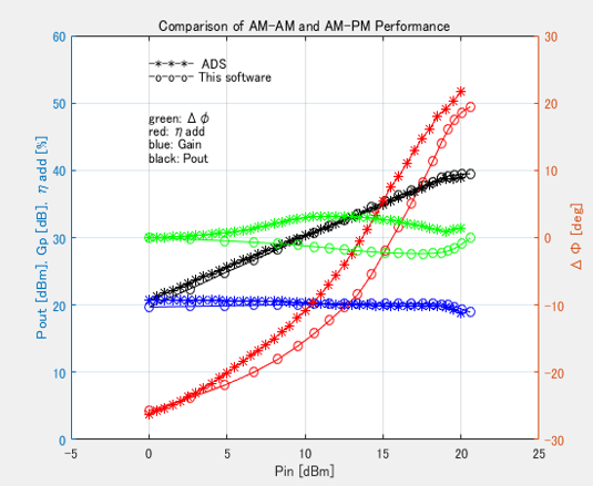
An L-Band 10W GaN HEMT amplifier using Cree GaN HEMT CGH40010 [16] has been designed. Power performances are compared by using the harmonic-balance simulator (ADS2022 Keysight Technology) [17] and this load-line analysis software, which is shown in Figure 15. Output power and gain are in good agreement. Power-added efficiency and insertion phase variation are slightly different. These results demonstrate that the load-line analysis software introduced here is a candidate for the nonlinear analysis of GaN HEMT amplifiers. To verify the validity of the load-line software, the L-band 10W GaN HEMT amplifier is due to be actually fabricated and measured hereafter.
4. Comparative Analysis
A comparative analysis of the load-line method used in the microwave power amplifier is summarized in Table 4. A low-frequency I-V load-line measurement setup is shown in [2] and [3] to analyze low-frequency dispersion phenomena of GaN HEMT devices. The Cripps load-line theory is slightly modified to meet with low-voltage devices such as CMOS in [18] and [19]. That is, a slope of the load-line is adjusted for high efficiency in accordance with the knee voltage. By tilting a slope of the load-line for each cell of the distributed amplifier, high power and high efficiency over several octaves have been obtained [20] and [21]. The load-line is carefully chosen to achieve low-distortion and high-efficiency for both carrier and peaking amplifiers of the Doherty amplifier [22] and [23]. It must be noted that not only the load-line is carefully investigated but also time-varying waveform is checked in these load-line analyses. Similar to [2] and [3], a low- frequency I-V load-line is used to evaluate performance degradation of microwave transistor [24]. In addition, dynamic load-line is used in the design of narrowband and broadband amplifier designs [25] and [26]. This work presented here is based on a load-line analysis software, which can provide linear/nonlinear power and distortion performances. Therefore, this software can be considered to be useful to analyze various nonlinear power performance described in these References.
Table 4: Comparative analysis of the load-line method for use in the power amplifier design

5. Conclusion
An advanced load-line analysis software for nonlinear circuit design and simulation of microwave low-distortion, high-efficiency and high-power GaN HEMT amplifiers has been presented. A single software package can incorporate DC, small-signal and large-signal performances of GaN HEMT devices, and then analyze nonlinear performance of AM-AM and AM-PM characteristics, and finally evaluate IMD and EVM. With the use of behavioral modeling, high speed and high accurate simulation become available. In addition, the software is based on a time-domain analysis using time-varying electrical waveform and thus can provide clear and deep insight into the nonlinear behavior of GaN HEMTs as well as the nonlinear circuit design of low-distortion and high-efficiency GaN HEMT amplifiers.
Acknowledgement
This research is based on a study commissioned by the National Institute of Information and Communications Technology, Japan (“Research and development on high-speed beam steering technology toward Beyond 5G” adopted number 06001).
- S. C. Cripps, RF Power Amplifiers for Wireless Communication, 1st ED., Artech House, Norwood, MA, USA, 1999; pp. 24-32.
- A. Raffo, F. Scappaviva, G. A. Vannini, “New Approach to Microwave Power Amplifier Design Based on the Experimental Characterization of the Intrinsic Electron-Device Load Line”, IEEE Transaction on Microwave Theory and Techniques, vol. 57, no. 7, July 2009
- A. Raffo, G. Bosi, V. Vadalà, G. Vannini, “Behavioral Modeling of GaN FETs: A Load-Line Approach”, IEEE Transaction on Microwave Theory and Techniques, vol. 62, no. 1, January 2014
- Focus Microwaves Data Manual. Montreal, QC, Canada: Focus Microwave Inc., 1988.
- J. M. Cusak, S. M. Perlow, B. S. Perlman, “Automatic load contour mapping for microwave power transistors”, IEEE Trans. Microwave Theory Tech., vol. MTT-22, no. 12, pp. 1146–1152, December 1974.
- J. C. Rodringues, Computer-aided Analysis of Nonlinear Microwave Circuits, 1st-ED., Artech House, Norwood, MA, USA, 1998; pp. 229-309.
- K. Mori, M. Nakayama, Y. Itoh, S. Murakami, Y. Nakajima, T. Takagi, Y. Mitsui, “Direct Efficiency and Power Calculation Method and Its Application to Low Voltage High Efficiency Power Amplifier”, IEICE Transaction, vol. E78-C, no.9, pp.1229-1236, September 1995.
- Y. Ikeda, K. Mori, M. Nakayama, Y. Itoh, O. Ishida, T. Takagi, “An Efficient Large-Signal Modeling Method Using Load-Line Analysis and its Application to Non-Linear Characterization of FET”, IEICE Transaction, vol. E84-C, no. 7, pp. 875-880, July 2000.
- Keysight Product Note 89400-14.
- MATLAB R2021B, Mathworks.
- T. R. Turlington, Behavioral Modeling of Nonlinear RF and Microwave Devices, 1st ED., Artech House, Norwood, MA, USA, 2000, pp. 107-133.
- W. R. Curtice, M.A. Ettenberg, “Nonlinear GaAs FET Model for Use in the Design of Output Circuits for Power Amplifiers”, IEEE Transactions on Microwave Theory and Techniques, vol. 33, no. 12, December 1985
- H. Statz, P. Newman, I. W. Smith, R. A. Pucel, A. Haus, “GaAs FET device and circuit simulation in SPICE”, IEEE Transactions on Electron Devices, 1987, vol. 34, No. 2
- H. Jiang, P. Gong, W. Xie, B. Chen, B, H. Ma, C. Yang, “EVM Measurement and Correction for Digitally Modulated Signals”, 2018 Conference on Precision Electromagnetic Measurements (CPEM 2018)
- MATLAB Communication Toolbox, EVM Measurement.
- CGH40010, Wolfspeed, A Cree Company, USA
- Keysight Advanced Design System 2021
- X. Du, C. J. You, M. Helaoui, J. Cai, M. Ghannouchi, “Evaluation of Knee Voltage Effect and Soft Turn-on Characteristic on the Load Modulated Continuous Class-B/J Power Amplifier”, 2018 IEEE MTT-S International Wireless Symposium (IWS) 2018.
- P. Sandro, J. E. Mueller, R. Weigel, “Extension of the Load-Line Theory by Investigating the Impact of the Knee-Voltage on Output-Power and Efficiency”, Proceeding of the European Microwave Integrated Conferences, pp. 488-491, 2013.
- M. Coers, W. Bosxh, “Analysis of Tilting Load-Line in AlGaN/GaN Broadband Uniform Distributed Amplifier”, Proceeding of GeMic, 2014.
- M. L. Salib, D. E. Dawson, H. K. Hahn, “Load-Line Analysis in the Frequency Domain Distributed Amplifiers Design Examples”, IEEE MTT-S Digest, pp. 575-578, 1987.
- J. Kim, J. Moon, Y. Y. Woo, S. Hong, I. Kim, J. Kim, B. Kim, “Analysis of a Fully Matched Saturated Doherty Amplifier with Excellent Efficiency”, IEEE Transaction on MTT, vol 56, no. 2, pp. 328-338, February 2008.
- M. A. Medina, D. Schreurs, I. Angelov, B. Nauwelaers, “Doherty Amplifier Design for 3.5GHz Wimax Considering Load Line and Loop Stability”, Proceeding of the 3rd European Microwave Integrated Conference, pp. 522-525, 2008.
- G. Bosi, V. Vadalá, R. Giofrè, A. Raffo, G. Vannini, “Evaluation of Microwave Transistor Degradation Using Low-Frequency Time-Domain Measurements”, 2021 XXXIVth General Assembly and Scientific Symposium of the International Union of Radio Science (URSI GASS)
- N. C. Miller, D. T. Davis, S. Khandelwal, F. Sischka, R. Gilbert, M. Elliott, R. C. Fitch, K. J. Liddy, A. J. Green, E. Werner, D. E. Walker, K. D. Chabak, “Accurate non-linear harmonic simulations at X-band using the ASM-HEMT model validated with NVNA measurements”, 2022 IEEE Topical Conference on RF/Microwave Power Amplifiers for Radio and Wireless Applications (PAWR)
- N. Poluri, M. M. D. Souza,” Ease of Matching a Load Line Impedance in a 25 W Contiguous Mode Class BJF−1 Broadband Amplifier”, IEEE Microwave and Wireless Technology Letters, 2023, Vol. 33, No.2.