DC/DC Converter by using FPGA
(This article belongs to the Section Electrical Engineering (ELE))
Export Citations
Cite
Barnawi, A. and Zohday, M. (2024). DC/DC Converter by using FPGA. Journal of Engineering Research and Sciences, 3(3), 13–18. https://doi.org/10.55708/js0303002
Amin Barnawi and Mohammed Zohday. "DC/DC Converter by using FPGA." Journal of Engineering Research and Sciences 3, no. 3 (March 2024): 13–18. https://doi.org/10.55708/js0303002
A. Barnawi and M. Zohday, "DC/DC Converter by using FPGA," Journal of Engineering Research and Sciences, vol. 3, no. 3, pp. 13–18, Mar. 2024, doi: 10.55708/js0303002.
This paper discusses FPGA technology and assesses how this technology can be implemented to eliminate voltage spikes. This study also evaluates how FPGA can be used to remove the static voltage errors from the DC/DC boost converter. This technology is used to remove the voltage spikes when the impedance load is changed instantly. The FPGA stands for field programmable gate array. This system is used to control the dynamic behavior of a such system in practice. Through the use of this FPGA technology, it is very easy to implement such control algorithms that can able to work in real-time, and also their sampling period is very low. The required output can be achieved through the parallel implementation of control algorithms. In this paper, there are some experimental results through the use of FPGA technology in boost converter.
1. Introduction
1.1. Background
The use of DC/DC converters in the field of electricals features prominently in applications such as the power supplies used in electronic circuits. The DC/DC converter is also used in DC electric motors and for converting high-level and low-level DC voltages. The load impedance can be changed using different capacitance and inductive loads. The condition in which the voltage overshooting occurs at the output of the DC-DC converters so this condition is not reliable for these converters and may cause damage to the other electrical appliances like the electric motor. Later on, whenever the sudden change in the output voltage occurs, this change occurs when the loading impedance changes. This is quite real whenever any voltage disturbance occurs in any electrical appliances due to voltage overshoot, so this FPGA technology covers that phase of voltage overshoot in any electrical system.
1.2. Conceptual Clarification
For the practical measurement, some experiments have been performed by making a model of a DC-DC boost converter and using FPGA technology. The model can be implemented through different impedances in the circuit. In MATLAB, different simulations have been proposed regarding this boost converter. In this report, some experiments have been proposed by using this concept.
2. Literature Review
According to the author Spino, he has proposed a work about the DC/DC boost converter this has to be done through the use of FPGA technology. A correct model for the DC/DC boost converter has been presented through FPGA technology implementation. The two hardware designs of the converter have been presented through different FPGA footprints. This explicit design of the buck-boost DC/DC converter has been designed and this design will help to allow efficient circuit implementation. In this paper, two controllers have been implemented on FPGA [1].
For the DC-DC converter, how feed-forward controller can be implemented? The conventional DC/DC converter topologies like buck, boost, Cuk and buck-boost converters have their controlling techniques for certain applications. The voltage regulator is used to maintain the constant volt- ages at the output of these converters whenever a current or voltage change occurs at the input of these converters. For this, a range of control techniques has been implemented for linear and nonlinear control of these converters. These controlling techniques are used to overcome the dynamic changes in the output of the system. These controllers can be classified as proportional, proportional-integral-dynamic, and also proportional-integral. These all controllers are used to control the active behavior of these converters. This linear control of the converter is not sufficient to face high changes in the line voltages and also in load current. But the nonlinear control techniques like the Fuzzy logic con- trol, genetic algorithm, Adaptive Neutral Network, and also many other controlling techniques are used to increase the performance of these converters. Many controlling tech- niques have been implemented through the use of FPGA technology.
For controlling the output voltage of these converters PID auto-tuning technique is used. This technique is used to control the DC/DC boost converters through the use of relay feedback techniques. The controller parameters are used to maintain the output level of these converters.
These parameters of the controllers are used to control the output of these converters. This controller parameter is tuned and used as the PID regulator. This technique is used to remove the effect of parasitic resistance and inductance in the output capacitor of these converters. That produces a lot of noise at the output of the DC/DC converter so by using this technique of feedback control through the PID controller this noise can be reduced easily.
The author Elshaer has proposed a control technique for the DC-DC boost converter that is a PID controller in a Photovoltaic system. This controller can be tuned with the help of a Genetic algorithm for the regulation of the output voltage. For tuning the proportional, integral, and derivative gain of this PID controller the Fuzzy-PID controller was used. For controlling the duty cycle of the boost converter, a smart controller was used in this research. For the fixed frequency at the input, a nonlinear controller was proposed. For the power amplifier, a four-switch non-inverting Buck- boost converter is used that is based on the sliding mode control strategy. The ideal advantage of using this controller is that this controller will help to increase the performance, efficiency, and energy of the system using these converters [2].
According to the author Fumio, he has designed a nonlinear controller called the fuzzy controller, and this controller is used to regulate a Cuk converter and also the boost converter. A complete study has been carried out for the output of these converters [3]. According to the author Gupta, he has proposed a fuzzy logic controller for controlling the output of the bulk and boost converters for a common algorithm of this converter. For the experimental implementation of this controller, an 8-bit microcontroller is used. This Fuzzy logic controller is used for the steady-state output of the boost converter [4].
Mattavelli describes the aim of the Fuzzy controller for the bulk-boost converter. In this research, the simulation results have been proposed and also proposed a control methodology. According to the author Raviraj, he has de- veloped a linear PI controller, fuzzy controller, and also the sliding mode controller [5].
In this paper, the author Tseng has proposed a high- performance design for the DC/DC switching power converter like the Boost converter. This converter is involved in providing a regulated voltage of 50 and a current of up to 15 amperes. For getting a high range of adjustable voltage at the output of the converter a PI gain control scheme has been designed through the use of an FPGA chip. In this paper experimental results also have been proposed. Through the use of FPGA technology, the issue of limited adjustable output voltage range for these PWM switching converters has been resolved. Also, this technique increases the efficiency of the output of the system. Using the ZVS technique, the output efficiency of the system improved [6].
According to the author Hyo-Sik, he has proposed a fuzzy controller for the boost and buck converter. And this can be done using a digital signal possessor whose processor is switched at 10 MHz frequency. Then after that, an integrated Fuzzy controller is designed and used for the boost converter control and this can be done through the current mode control technique [7].
3. Mathematical Model of the System
3.1. DC/DC boost converter
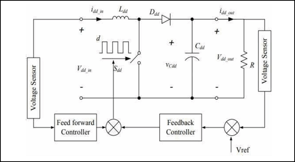
The DC/DC converter is shown in the figure 1.
3.2. Parameters of the DC/DC Boost Converter
For the parameter first of all there is a demonstration of the specifications of the DC/DC boost converter. The input voltage of the converter is set to 400 volts. The inductor, capacitor, and load resistor values are calculated through their formulas. The inductor value is 2.9 × 10⁻³. For the setting of IGBT FET resistance is 0.1 and put the snubber capacitance at infinity. For the setting of the diode of the boost converter, the resistance is set at 0.001, the snubber resistance is set at 500, and the snubber capacitance is at 250 × 109. The capacitor for the boost converter is set at 1× 10⁻⁶ the value of the load resistor is set at 20 ohms and the value of the boost converter is not according to the requirement that has been set in the problem. Based on these specifications, the parameters for the DC/DC boost converter have been calculated.
The switching frequency of this power-rated boost converter is set to 5 kHz. For finding the inductance value, in the first step find the resistances value according to the diagram and then calculate the value of the duty cycle ratio. After this find the rated input current of the inductor. Then through the input current ripple, the value of the inductor used for this boost converter can be found easily. The capacitor value of this boost converter can be calculated through the output voltage ripple ratio. The peak switch voltage is equal to the input voltage for this boost converter. The current value of this power diode is 150 A. The phase change in the circuit is measured by the IBC circuit design using MATLAB/Simulink software.
3.3. Design of Feed Forward Control
The DC/DC boost converter is very important in the field of electrical like the electric motors are controlled through these converters. The feed-forward controller has been designed for the DC/DC boost converter. This feedback controller has been designed by measuring open loop line regulations that are for the fixed load and can be set up to 5 percent and the DC input voltage can be changed by 400%.
After using this converter, the load regulation was also good without the use of a negative feedback loop.
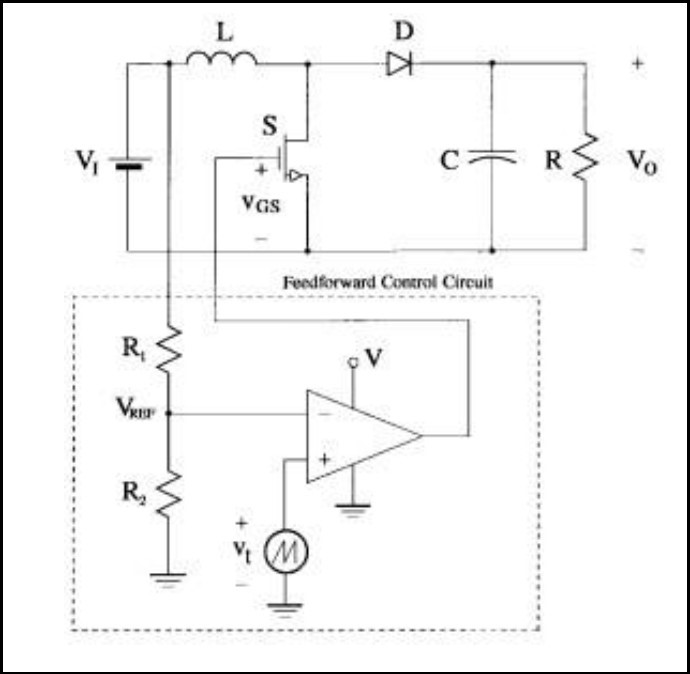
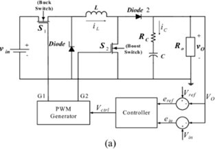
The feed-forward control of this converter consists of a comparator. The voltage divider for this controller is composed of two resistors that are R1 and R2 and the comparator for this controller is an operational amplifier that is supplied by only a single voltage source V. The vt is the sawtooth and this voltage is applied at the non-inverting input of the comparator. The peak value of the Sawtooth of voltage is denoted by VT M and this value is set up to 5-10 voltages. The switching frequency of this converter is set according to the frequency of the saw tooth voltage. For the input of this comparator, the reference voltage is applied as the inverting input of the comparator. And this reference voltage is denoted by VREF. This reference voltage can be written as
$$V_{REF} = \frac{R2}{R1 + R2} * V1 \;\alpha V1 \tag{1}$$
In the equation the \(\alpha \frac{\text{R2}}{\text{R1} \, \text{R2}}\) the output of this comparator is like a rectangular wave and this wave is used as the gate to source the voltage of the MOSFET. For increasing the output current of the rectangular wave and this wave is used as the gate to source the voltage of the MOSFET. For increasing the output current of the comparator, for this, attach the non-inverting buffer between the power MOSFET and the comparator [8]. For this, the on-duty cycle of the power transistor can be defined as
$$D = \frac{t_{on}}{T} \tag{2}$$
In this equation, the ton is the period when this power MOSFET is on and the period of this is equal to T 1t
The prototype of the system that will be implemented using MATLAB Simulink [9] is shown in figure 2 The IBC system development is based on the desired objectives and produced an output voltage that is approximately equal to the desired voltage. The conventional boost converter indicates higher efficiency, high reliability, low ripple current, and lower voltage ripples.
$$\frac{VTM}{T} = VREF \left[(1 – D)T\right](1 – D)T\tag{3}$$
$$V1 \left[(1 – D)T\right](1 – D)T * \frac{\text{R2}}{\text{R1 R2}}\tag{4}$$
After arranging these values this can be written as
$$D = \frac{VREF (1 – D) T}{VTM}\tag{5}$$
$$\alpha * \frac{V1 (1 – D) T}{VTM}\tag{6}$$
The output voltage of this feed-forward controller can be found as
$$V_o = \frac{1}{1 – D} * V1 \tag{7}$$
Through the substitution of the values, the output volt- age can be written as
$$V_o = \frac{VTM}{\alpha} \tag{8}$$
$$V_o = \left( \frac{R1}{R2} + 1 \right) * VTM \tag{9}$$
The operational amplifier can be used as the comparator when its slew rate is high enough and the slew rate can be found by assuming the value of the rise time and fall time of the gate-to-source ratio. The slew rate of the operational amplifier can be calculated.
$$SR = \frac{\Delta V_{GS}}{t_r} \tag{10}$$
$$SR = \frac{20\Delta V_{GS}}{T} \tag{11}$$
$$SR = 20 f_s \Delta V_{GS} \tag{12}$$
In this equation, the ∆VGS is the peak-to-peak voltage from the gate to the source voltage [10].
For designing the control system for this boost converter set the voltage reference at 1 and for designing the PID controller set the proportional part of the PID controller at 0.7, the integral part of the PID controller is set at 100, and for the advanced setting of this controller. The upper saturation limit is set at 1 and the lower saturation limit at 0.1. Attached are the DC-DC PWM generator setting the switching frequency at 5000 and the sampling time up to 1× 10⁻⁶.
The operational amplifier can be used as the comparator when its slew rate is high enough and the slew rate can be found by assuming the value of the rise time and fall time of the gate-to-source ratio. The slew rate of the operational amplifier can be calculated.
4. Simulation Results
MATLAB/Simulink platform is used to perform the simulation of the DC-DC boost converter. The simulation results showed that the proposed converter configuration has higher energy productivity compared to traditional converter designs.
The design of the boost converter is implemented on MATLAB Simulink is shown in figure 3.
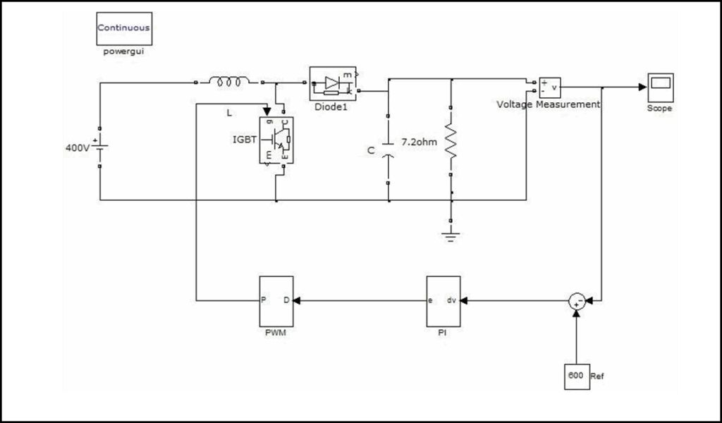
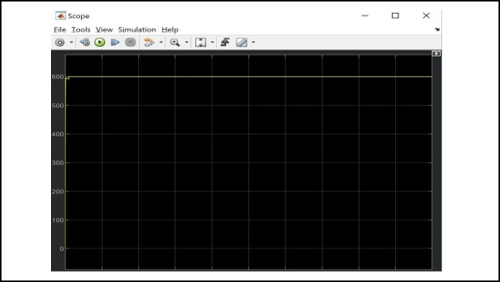
The voltage waveform of the boost converter can be seen through the help of the scope. The voltage is regulated by changing the duty cycle. Figure 4 shows the produced signal by using the waveform Editor (*.vwf). In the present situation, the time for on-off switching is considered to compare with the calculated values.
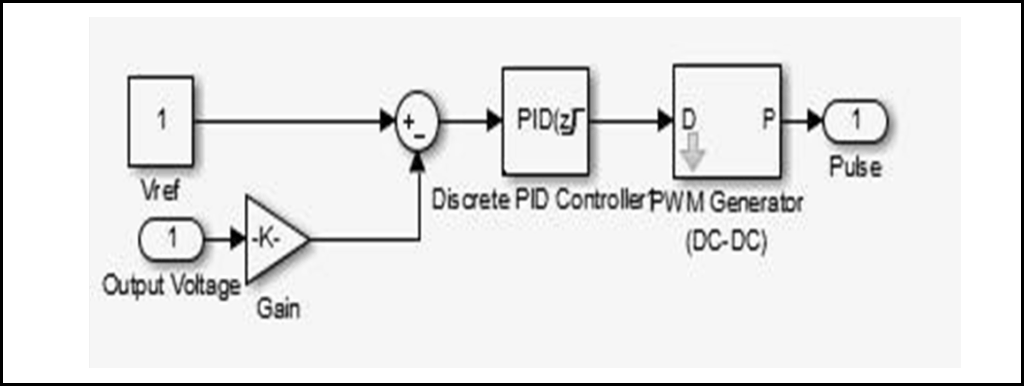
The inside of the feedback controller is like that by set- ting the gain value of 1/20 the design of the controller is like. The controller diagram is shown in the figure 5.
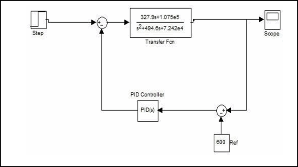
The system with the calculation of the transfer function was modeled in Simulink for control form as shown in Figure 6.
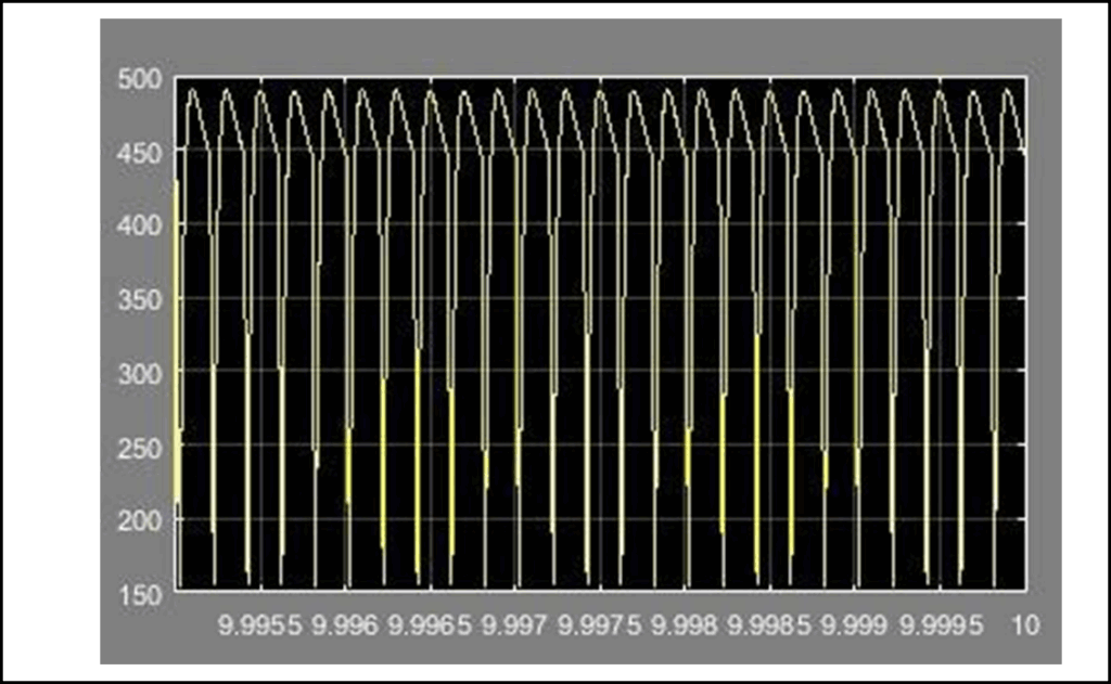
The voltage waveform after attaching the feed-forward controller the output voltage is also almost according to the requirement. The figure depicts output voltage that is slightly different from the calculated values. the control of the duty cycle on both sides of the whole phase is related to the change in voltage. The controllable output voltage is demonstrated is shown in figure 7.
5. Development of an FPGA-Based Controller Algorithm
A block diagram as shown if figure 8 shows the required process to develop the FPGA controller algorithm. It starts with writing Verilog code for the switching controller, which describes how the controller works it should meet the hard- ware requirements. After that, with good verification assign the I/O pins, because any mistake in this will affect the downloading of the code to the FPGA board. Finally, implement the hardware to verify that the controller code design successfully does its function.
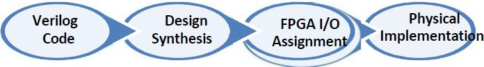
Figure 8: Voltage Output
The relationship between the output voltage to the input voltage and duty cycle (D) is described in the following table.
Table 1: Relationship of output and input
Converter Equation | Output Voltage Style |
Buck | Vout = Vin * D |
Boost | Vout = Vin/(1-D) |
6. Case Study Non-Inverting Buck-Boost Converter
Here we have chosen a Non-Inverting Buck-Boost converter as a case study to implement the FPGA control algorithm the figures 9 and 10 shows how the circuit looks like.
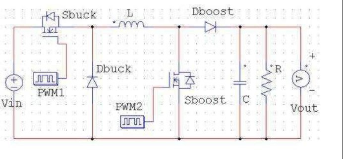
Figure 9: Circuit 1
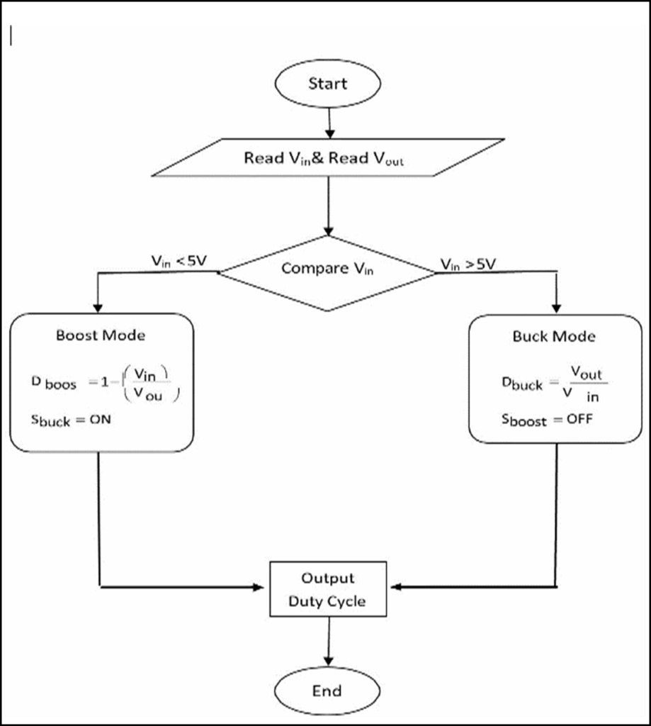
So now from the table and the figure it is clear the relationship between Vin, Vout, and D (duty-cycle) is. It is also obvious from the equations in the previous sections we can start to make the flowchart of the control algorithm as shown in the figure 11.
So now we got our flowchart which describes how the process flows to give us our control algorithm. The Verilog code of the voltage control loop is as follows.
module Voltage_control_loop (Vin, Vout, Dboost, Dbuck); input [2:0] Vin, Vout; output [4:0] Dboost, Dbuck; reg [4:0] Dboost, Dbuck; always @(Vin or Vout) begin
if (Vin < 5)
Dboost=1-(Vin/Vout); else Dbuck=Vout/Vin; end module
6.1. Simulation of the Voltage Control Using Cadence Software
Starting to check if the algorithm we developed successfully controls the voltage as we want, we simulate our algorithm using cadence software as shown in figure 12.
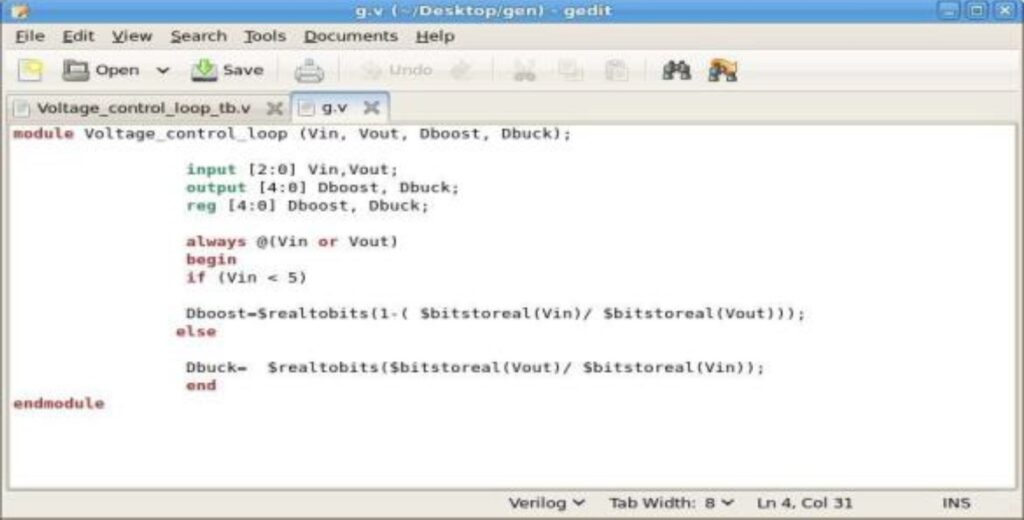
Figure 12: Veilog code
After writing the Verilog code in cadence and did run it, we got the following result as shown in figure 13.

7. Conclusion
It is concluded that boost converters are very valuable for electrical applications. For removing the ripples at the output of the boost converter a control technique can be implemented that is used to remove the voltage spikes from the output of the boost converter. In this report, a system is implemented for removing the line variation and the variation at the output of the boost converter can be done. For removing these errors at the output, a technique of feed-forward controller is used as the feedback of this boost converter. For setting the value of the parameters of the boost converter a feedback controller can be designed. In this report, the parameters for the feed-forward are designed by setting the values of input voltages. For this report, it can be seen that the line voltages are quite better when the high load impedance is implemented. At the output of the load regulation, load regulation is perfect at the output of the boost converter. Also, in this report, we showed how to develop a control algorithm using FPGA technology. The algorithm was implemented and tested and it works well but it has to be tested in real hardware to verify its efficiency and figure out any issue to be solved.
- V. Spinu, A. Oliveri, M. Lazar, and M. Storace., “FPGA implementation of optimal and approximate model predictive control for a buck-boost DC-DC converter.,” In Control Applications (CCA), 2012 IEEE International Conference on IEEE, pp. 1417- 1423, 2012, DOI: 10.1109/CCA.2012.6402444
- M. Elshaer, A. Mohamed and O. A. Mohammed., “Smart optimal control of DC-DC boost converter for intelligent PVsystems,” In Intelligent System Application to Power Systems (ISAP), 2011 16th International Conference IEEE, pp. 1-6, 2011, DOI: 10.1109/TDC-LA.2010.5762913
- T. I. I. O. a. M. S. F.Ueno, “Regulation of Cuk converters using fuzzy controllers,” In Telecommunications Energy Conference, 1991. INTELEC’ 91., 13th International, IEEE, pp. 261-267, 1991.
- R. Gupta, R. G. Lamba, and M. I. G. Singh, “A Comparative Study of Conventional and Fuzzy Logic Control of DC Drive with Power Factor Correction,” PhD diss, 2012.
- P. Mattavelli, L. Rossetto, G. Spiazzi and P. Tenti, “General-purpose fuzzy controller for DC-DC converters.,” IEEE Transactions on Power Electronics, 1997, vol. 12, no. 1, pp. 79-86,
- K-H.Tseng and C.-L. Chen, “Design and hardware implementation for a full-bridge phase-shift PWM DC/DC converter system with FPGA-based PI gain-scheduling control.,” In Industrial Electronics and Applications (ICIEA), 2011 6th IEEE Conference on, IEEE, pp. 1578-1582, 2011, DOI: 10.1109/ICIEA.2011.5975842
- H.-J. K. Hyo-Sik Park, “Simultaneous control of DC-DC converters by DSP controller,” ICPE (ISPE), pp. 203-207, 2001.
- C. Yao, X. Ruan,W. Cao and P. Chen., “A two-mode control scheme with input voltage feed-forward for the two-switch buck-boostDC–DC converter.,” EEE Transactions on Power Electronics, 2014 vol. 29, no. 4,
pp. 2037-2048, DOI: 10.1109/TPEL.2013.2270014 - P. Karamanakos, T. Geyer and S. Manias., “Direct voltage control ofdc–dc boost converters using enumeration-based model predictive control,” IEEE Transactions on Power Electronics, vol. 29, no. 2, pp.
968-978, 2014, DOI: 10.1109/TPEL.2013.2256370 - J. C. Rosas-Caro, J. M. Ramirez, F. Z. Peng and A. Valderrabano, “A DC-DC multilevel boost converter.” IET Power Electronics, pp. 129-137, 2010, DOI: 10.1049/iet-pel.2008.0253