An Educational Exhibit Aimed at Demonstrating the Rate of Growth of Computer Technology to Graduate Students
(This article belongs to the Section Information Systems – Computer Science (ISC))
Export Citations
Cite
Bucci, G. and Zaza, I. (2024). An Educational Exhibit Aimed at Demonstrating the Rate of Growth of Computer Technology to Graduate Students. Journal of Engineering Research and Sciences, 3(11), 1–23. https://doi.org/10.55708/js0311001
Giacomo Bucci and Imad Zaza. "An Educational Exhibit Aimed at Demonstrating the Rate of Growth of Computer Technology to Graduate Students." Journal of Engineering Research and Sciences 3, no. 11 (November 2024): 1–23. https://doi.org/10.55708/js0311001
G. Bucci and I. Zaza, "An Educational Exhibit Aimed at Demonstrating the Rate of Growth of Computer Technology to Graduate Students," Journal of Engineering Research and Sciences, vol. 3, no. 11, pp. 1–23, Nov. 2024, doi: 10.55708/js0311001.
This paper is an extended version of that presented at the conference Histelcon 2021 (IEEE). It provides a deeper illustration of the elements of the exhibit under development at the Faculty of Engineering at the University of Florence (Italy). The paper presented at Histelcon 2021 focussed on the birth of microprocessors, on the 8086, on an example of core memory and punched tape. In the following, though these arguments are still dealt with, much material has been added, including electromechanical calculators, medium-sized computer systems, personal computers, 8-bit microprocessors, disks, and other elements on the exhibit. The organization of the paper is quite different. It starts with a description of old computing machines (including a slide rule) before passing to the illustration of some more recent computer systems. The last part of the paper is dedicated to the illustration of the mentioned elements. Though there are many computer museums around the world, usually open to the general public, this exhibit is directed to the students of the Faculty, to enlighten the pace of development in computers.
1. Introduction
At the School of Engineering of the University of Florence (Italy), a sort of museum of Computers is being set up. Transliterating the Italian name, the exhibitwould be named “An exposition path through technology”, just to point out the pace of technology growth. The aim is to make it clear to the students, essentially young people, how the rate of improvement has been impressive. While there are many computer museums [1] for the general public, this exhibit is directed to the students of the Faculty.
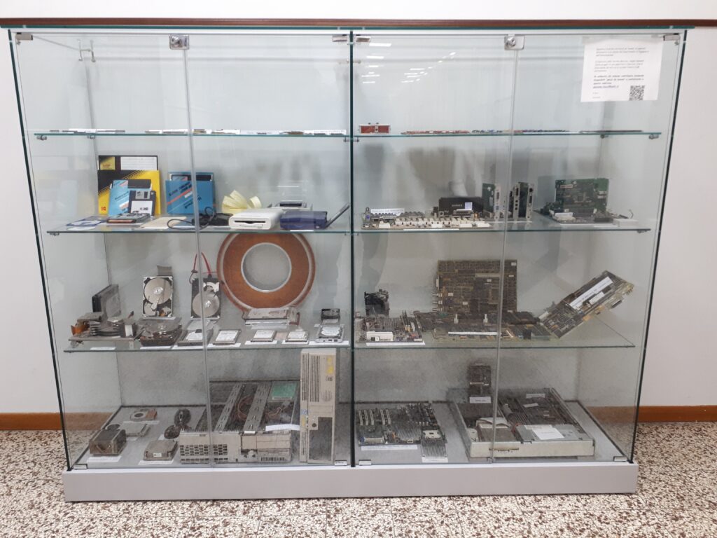
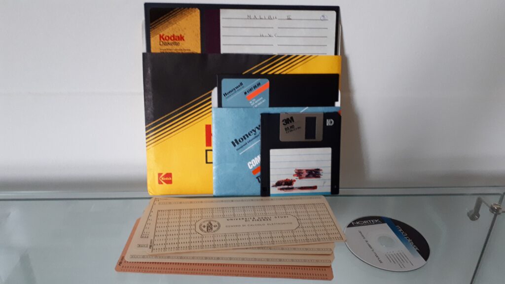
The exhibit is made up of some display cabinets where the various pieces are exposed. These include microprocessors, memories, disks, personal computers, both desktop and laptop, as well as some (parts of) systems of medium and low size. An example of a display case is in Figure 1. Most of these objects come from the same School of Engineering in Florence, where, at the end of their usage period, they were declared down and made available. Some materials come from private individuals.
Microprocessors are by far the largest class of devices. Unfortunately, the first microprocessor in history, the Intel 4004 [2, 3], is not available at the moment; on the other hand, there is the 8008, a 8-bit microprocessor, Intel’s second micro. Though the largest class of microprocessors belongs to the X86 family, there are also devices from other manufacturers (AMD, Motorola, Zilog, and others). Several types of memory are on display, including a magnetic core memory that is presumably part of an Olivetti Elea computer. The auxiliary storage devices section is also well stocked, including an interchangeable plate of a 14″ hard disk drive, plus numerous disk drives of different generations. Among the devices on display, there is no shortage of complete systems or parts of systems. The collection includes a variety of personal computers: from the first 8-bit devices (ZX Spectrum, Olivetti M10, and others) to modern laptops.
As a complement to the exhibit, a document (in Italian, about 150 pages) [4], downloadable from the Internet, is provided; it contains a more detailed exposition of the exposed elements. It has a chapter entitled “How a laptop can be disassembled and re-assembled”. The document is regularly updated when new pieces are added. It aims to be an instructional aid for the students of Information Technology, Electronics, and Telecommunications. We hope that this document can be useful to those who, not being specialists in the subject matter, will find information in it that is not always easily available. Of course, the document is downloadable from the Internet, at the address https://sites.
google.com/unifi.it/calcolatori-elettronici.
The objects described in the rest of this article are a subset of those on display. We illustrate the specimens of the greatest historical value and/or the elements that have had an important technological impact. The description accompanying them is essentially the same as that contained in the explanatory leaflet [4], though certain general considerations have been omitted. Part of the following has been already presented in [5].
2. Mechanical, electromechanical and electronic calculators
The exhibit contains some old calculating machines. In the following, we begin with a slide rule, then a couple of electromechanical machines are described, plus a couple of electronic calculators.
2.1. Slide rule
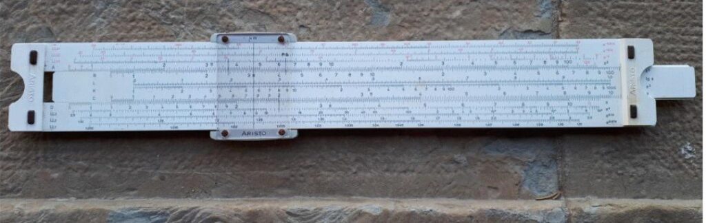
Until the advent of pocket electronic calculators, the slide rule was the calculation tool of choice for the technical- scientific community. In its pocket form, it often peeked out from the breast pocket of engineers’ jackets. The ruler allows, with a few maneuvers, calculation of multiplications, divisions, squares, cubes, exponentials, and some trigonometric operations. It is based on the properties of logarithms. Since the logarithm of the product is equal to the sum of the logarithms of the two factors [log(xy)=log(x)+log(y)], it follows that if the numbers are represented in a logarithmic scale their product is obtained by positioning in a sum fashion the two logarithmic scales on which the numbers are represented. To this end, the slide rule is made up of three elements: (i) a body on which there are fixed scales; (ii) a sliding ruler, inside the body, also provided with numerical scales; (iii) a cursor with one or more reference lines.
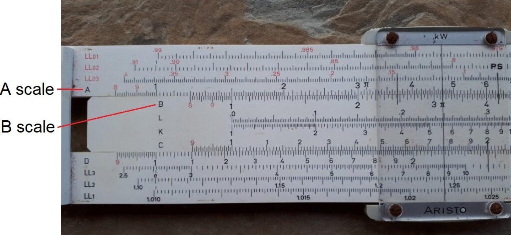
The image of Figure 2 shows the rule with the sliding rod positioned so that the 1 of its upper scale (scale B) corresponds to the 1.5 of the adjacent fixed scale (scale A) . The result of the products, 1.5 × 2 = 3 and 1.5 × 3 = 4.5, can be read on the A scale in correspondence with the 2 and 3 on the B scale.
In the close-up image of Figure 3, the cursor is positioned on π of scale B, in order to facilitate reading the result of the product 1.5π = 4.7 on scale A. Obviously, all results are to be considered approximate unless it is obvious that we are dealing with products that give an exact result (as in the preceding examples).
The first slide rule is attributed to the Englishman William Ougthred (1575-1660), who built a model composed of two rulers in 1622, based on the studies of John Napier (1550-1617).
Starting from 1970, with the advent of affordable pocket electronic calculators, the slide rule was abandoned by the technical-scientific community. Not only because it provides approximate results, but also because it does not allow addition and subtraction operations, which any trivial calculator does. The German city of Darmstadt had a centuries-old, thriving slide-rule manufacturing industry. With the arrival of pocket computers, this industry disappeared in a few years. Production of the slide rule ended around 1978.
2.2. Monroe LA7-200 calculating machine
In 1820 the Frenchman Charles Xavier Thomas de Colmar built the first completely mechanical calculating machine, called Arithmomètre. Unlike the prototypes of Pascal and Leibniz a century before, it was a commercial product. Towards the end of the 19th century, other manufacturers entered the market. The Monroe Calculating Machine Company was founded in New York in 1912 by Jay R. Monroe.
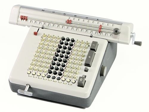
The Model LA7-200 is an electromechanical calculator, capable of performing the four fundamental arithmetic operations (addition, subtraction, multiplication, and division). It was produced by the Dutch branch of Monroe in 1950. You can set numbers of (up to) 10 digits on the keypad. Internally there are 10 counters and 20 accumulator registers. The results appear in the cart (two distinct lines depending on the operation). The trolley crank is used to reset it. The machine weighs 7.6 kg. A video on its functioning can be found at the address https://www.youtube.com/watch?v=HFGcv7a8l5M.
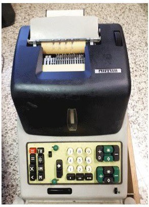
2.3. The Olivetti Tetractys calculating machine
This electromechanical computer was introduced in 1956 together with the Divisumma 24, from which it was derived, with some extensions, including a double totalizer. It performed the basic arithmetic operations. The keyboard had 10 digits in addition to the keys for the calculation functions; the printing was on a roll of scrolling tape. Tetractys represented the state of the art of mechanical calculation of those years. The two totalizers allowed moving from one operation to the next while preserving the products and quotients of the previous calculation.
The dimensions are 24; 42; and 24.5 (W; D; H) centimeters.
It weighs 15kg.
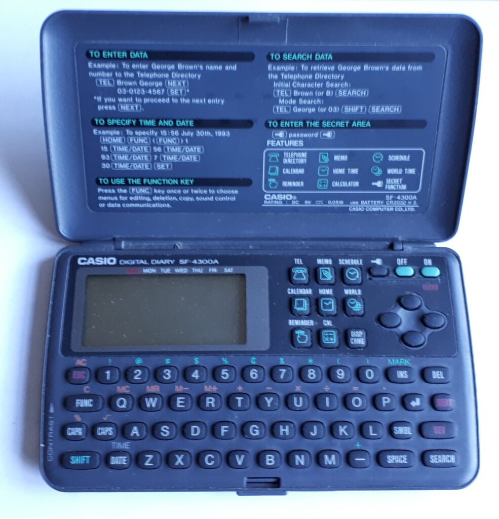
2.4. Casio Digital Diary SF-4300A
The Casio SF-4300A is a rather rudimentary device (Figure 6), with a few more features of a calculating machine. The SF-4300A was marketed started in the early 1990s. It had one memory of 32 kB and could perform the following functions: (corresponding to the same number of buttons located to the right of the display): phone book; storing texts and other data (memos); to-do list (schedule); calendar; clock (local and world); alarm (reminder); calculation.
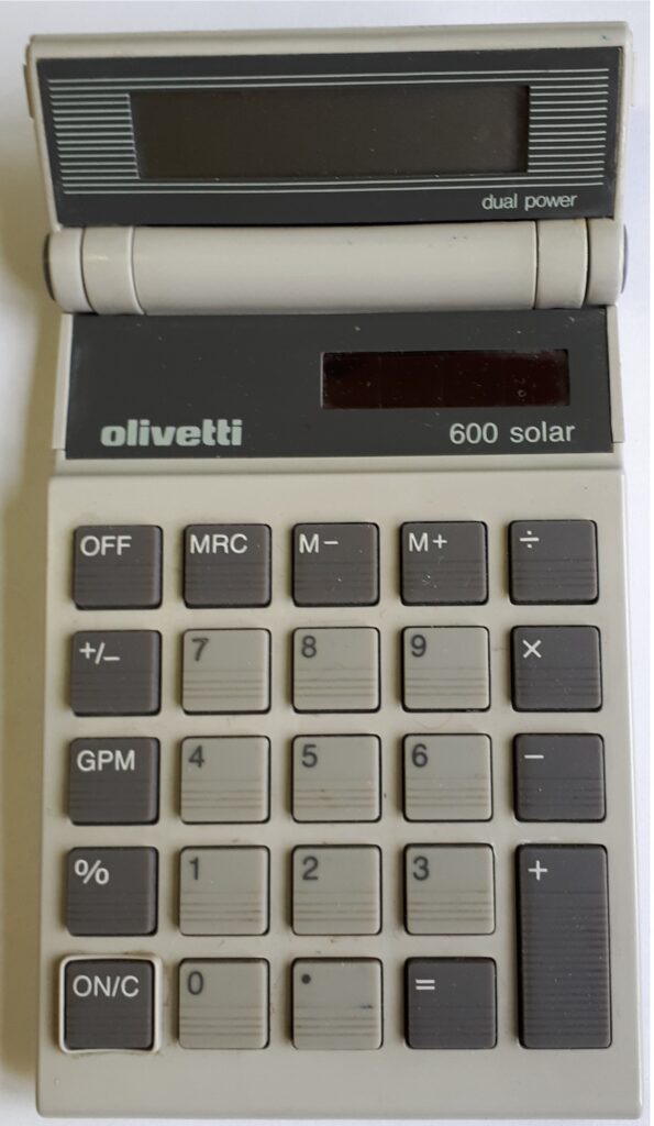
2.5. Olivetti 600 Solar
The Olivetti 600 Solar (Figure 7) was introduced in 1989 (approximately). It is a small pocket electronic computer (125x82x15mm), whose main feature is that it is equipped with solar cells which allow its use in practically any light condition. The display is liquid crystal.
Electronic calculators equipped with solar cells began to appear in the late 1970s. But they have not achieved great success, probably because the always lowering consumption of electric devices does not make the presence of solar cells important. Similar calculators are currently on sale at a cost of around ten dollars. However, there is a more reason that makes use of electronic calculators unattractive: any mobile phone has at least one App that carries out the operations of such calculators.
3. Portable computers
There are almost thirty portable computers on display. Here we present a selection: the Sinclair ZX Spectrum, the Commodore 64, the Olivetti M10, the Toshiba T1600, the Compaq Contura Aero 4/33c, the Apple PowerBook G4,
3.1. ZX Spectrum
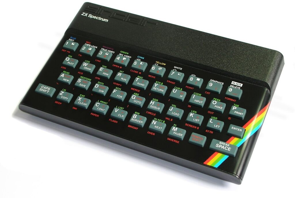
The ZX Spectrum was a family of small portable computers (23.3 × 14.4 × 3 cm), introduced by Sinclair in 1982 and produced until 1986 by the same manufacturer, and, from 1986 to 1992, by Amstrad.
The ZX was based on the Z80 microprocessor. In the initial version at 3.5 MHz, with a RAM of 16 kB, was man- aged through a sort of operating system called Sinclair Basic, essentially a version of Basic to which some commands such as RUN for starting programs had been added. The version on display is the ZX 48K model, i.e. with 48 kB of RAM. The ZX has been very succesful: 5 million of the ZX Spectrum have been sold worldwide, not counting imitations.
Although the ZX Spectrum is no longer produced, small cards are on sale which allow the implementation of a ZX Spectrum, and other various small computers in the same category as the ZX. Figure 8 shows one such small card the ZX-Uno (V4.1). The card size is 86 by 56 millimeters. It is preferentially oriented towards the creation of the ZX. But it also allows the construction of the Apple II, the VIC-20 (Commodore), the Acorn Atom, the Atari 2600, and many others. Anyway, this requires an appropriate setting of an FPGA (Field Programmable Gate Array), which can be defined via VHDL or Verilog languages.
The top image of Figure 9 shows the board without components; the image in the middle the placement of the connectors, while the lower the mounted components. Basically, anyone who wants to build one ZX Spectrum just needs to assemble the required components, connect a key- board, a television (depending on the video), and connect the power supply (via USB).
3.2. Commodore 64
Produced by Commodore Business Machines, from 1982 to 1994, the Commodore 64 (C64, 64 indicates 64 kB of memory, Figure 10) was a very successful product. 17 million units were sold, surpassing the sales numbers of the Apple II and other personal computers very popular at the time (including, in Europe, the ZX Spectrum).
The C64 was the first truly mass-market PC, thanks to its affordable price and high performance. It was marketed with an aggressive pricing policy: it was sold in department stores and even toy stores. The C64 looks like a headboard, quite massive by today’s standards, in Italy was called “Biscottone” (big cookie). On the back, there were connectors for audio cassettes, serial or parallel printers, and TV sets (as video output).
The processor was an MOS 6510 from MOS Technology, operating at a frequency of approximately 1000 Hz to adapt to both the American and European television standards (1023 Hz for NTSC, 985 Hz for the PAL).
The 6510 was a 40-pin DIP (Dual In-line Package) IC. It was a derivative of the 6501, an 8-bit microprocessor that appeared in 1975 and was designed by a couple of engineers who had participated in the development of the Motorola 6800. The 65xx family processors were produced by several electronics industries and had considerable success. The 6501 had a bus compatible with that of the 6800, but a simplified internal architecture and instruction set. At the time the 6501 was introduced, while the Motorola 6800 was selling for $300, the 6501 was selling for $25 – consequently, Motorola had to lower the price to $35. The successor to the 6501, the 6502, was widely used, for instance, in the Apple II.
From 1985 to 1989 the Commodore C128 was produced (128 kB of memory and 8502 microprocessor, a higher performance version of the 6510), but it was not so successful: the era of 16-bit microprocessors had begun.
3.3. Olivetti M10
The Olivetti M10 (Figure 11) was introduced in 1983 and withdrawn in 1985. It employed an 80C85 CPU at 2.4 Mhz, CMOS version of Intel’s then widespread 8085.
The LCD had 8 lines of 40 characters (240 x 64 pixels, black and white); the keyboard with 94 keys it had the QZERTY layout (Italian layout used by Olivetti on its typewriters). It used a proprietary operating system from Microsoft, equipped with Basic, a word processor, an agenda, an address book, and Multiplan (Microsoft’s first spread- sheet before Excel), all on ROM. It is said that Bill Gates participated in the development of the programs and that this was the last time he directly programmed.
The RAM was static (non-volatile) 24 kB, and served as mass storage, but to be able to run Basic it was necessary to expand it to 32 kB. The M10 featured an RS232C serial port 25-pin, a 26-pin Centronics parallel port, and a connector for an external cassette recorder. Consumption was low enough to be powered by 4 normal 1.5V AA batteries. It cost from a million Lire to around 2.4 million Lire (today 1 million Lire corresponds to about =C500) for the most equipped version. It had the dimensions of 30x21x5 cm and weighed 1.7 kg.
At the time, “lightweight” laptops weighed just under 10kg, were extremely bulky, and had to be attached to the power socket. These factors, together with the captivating aesthetics, determined its immediate success. In numerical terms, sales in 1984 amounted to approximately 24,000 pieces; on the Italian market, the M10 reached 70% of laptop sales and 22% on the European market. It went out of production the following year when sales dropped dramatically. It is interesting to note that the M10 was the Olivetti version of the Kyotronic KC-85, a portable introduced in 1983 by the Japanese Kyocera. Probably the first real laptop. Three industries: Olivetti, Tandy, and NEC, had obtained the license to produce their own version of the Japanese laptop; Tandy operated on the American market, NEC on the Asian, and Olivetti in Italy and Europe.
3.4. Toshiba T1600
The Toshiba T1600 (Figure 12) was introduced in 1987. it was based on the 80C286 processor at 12 MHz. Memory was expandable to 5 MB. It could mount a hard disk of either 20 or 40 MB, plus a 3.5” flexible disk with 1440/720 kB capacity. It had an EGA standard video (16 colors from a palette of 64 and a resolution up to 640×350 pixels. MS-DOS was the operating system, but it was possible to install Windows 3.0. Its weight was 5.2 kg (with only one battery installed).
Suggested retail price was $5,000.
Figure 13 shows the components standing under the keyboard. The keyboard was easily removable and was connected via a flat cable to the indicated connector; a connector was also provided for mounting a possible memory expansion.
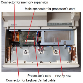
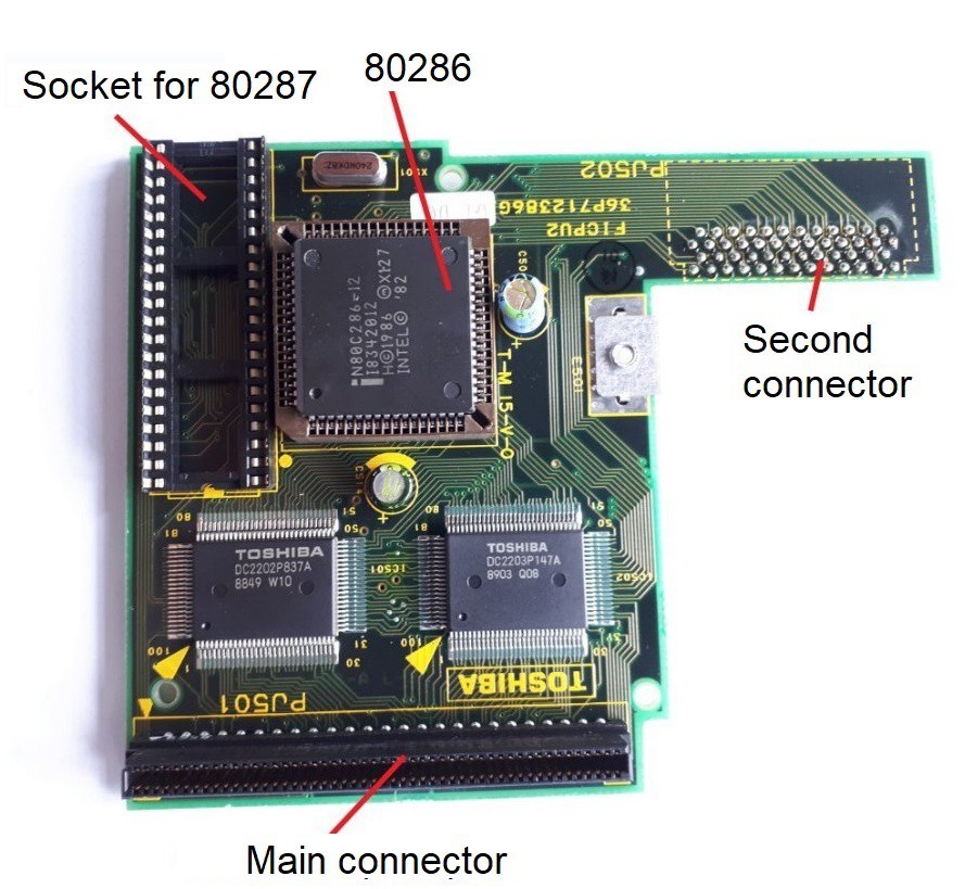
The microprocessor was mounted on the board which appears upside down in Figure 14. In turn, this card was mounted via two connectors on the system board (the second connector is seen from the soldering side in Figure 14); on this board, there was an empty socket for the insertion of the 80287 coprocessor.
A comment from back then: The T1600 is a truly portable machine; the enlarged backlit Supertwist EGA display is a marvel of readability.
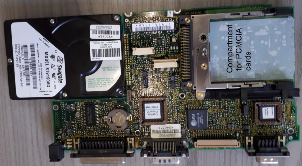
3.4. Portatile Compaq Contura Aero 4/33c
The Compaq Aero line was produced in various versions, with different processors, disks, and memories from the second half of the 1980s until around the mid-1990s.
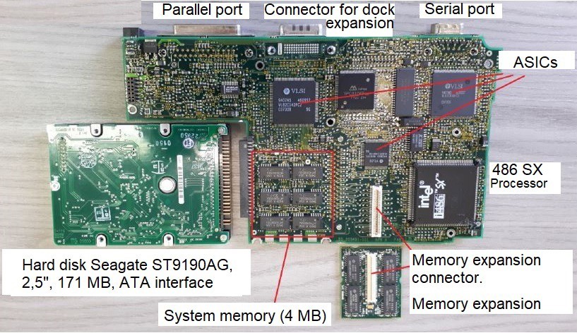
The model on display (Figure 15) has these characteristics: Intel 486SX processor at 33-MHz, with 8 KB of integrated cache; 8” monochrome display; 4 MB RAM, expandable to 20 MB; 171 MB hard drive (Seagate ST9190AG). Size was 19.5 x 26.7 x 4.3 cm, while it weighed less than 2 kg.
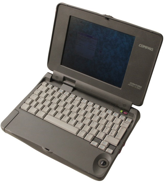
Furthermore, this laptop was equipped with a PCMCIA card that allowed the connection of an external 3.5-inch, 1.44 MB floppy disk. In subsequent models, the PCMCIA interface was replaced by a USB interface, the newborn industrial standard. The characteristic of the Compaq Aero was the trackball that can be seen on the right under the keyboard, together with the two buttons, barely visible in the photo on the right side (opposite the shift key). The trackball and the two buttons acted as the mouse.
3.5.1. The motherboard of the Compaq Contura Aero 4/33c
Figure 16 shows the motherboard from the side that, when mounted, looked downwards; Figure 17 the other side.
On the side facing downwards, there is the processor, the system memory, and a series of ASICs (Application Specific Integrated Circuits) devices, used by the manufacturer to implement accessory functions. The memory expansion was piggyback-mounted on the motherboard, it used eight 1M by 4 bits Hitachi HM514400B/BL ICs, for a total of 4MB. There was also a connector for dock expansion.
On the side facing upwards is the slot for the PCMCIA card.
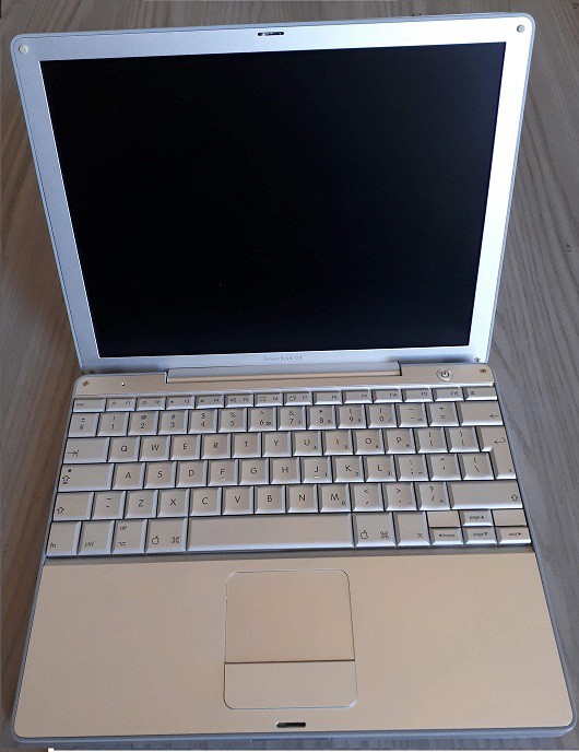
3.6. Apple PowerBook G4
The PowerBook G4 family was produced from 2001 to 2006. The family included a large number of performance models starting from the one produced in 2001. The acronym G4 indicates that the family uses PowerPC G4 processors. The one on display is the A1010 model introduced in January 2005.
The microprocessor was a PowerPC G4 (mod 7447) at 1.33 GHz, with 256 MB of RAM, and 256 kB L2 Cache. The hard disk had a capacity of 60 GB. The video was a 12″ with 1024×768 pixels. Dimensions 3×27,7×21,8 cm; weight was
2.1 kg.
The PowerBook G4s were the last Apple laptops to use PowerPC processors (see the discussion at the last paragraph of section 4.3).
4. Desktop computers
In the following some desktop computers, out of those in the exhibition are described.
4.1. Olivetti M24 New P100
Olivetti’s M24 line was introduced in 1983. Olivetti had previously produced the M20, based on a Z8000 processor and with its operating system. The M20 did not hit the main- stream market, which then, as now, was oriented towards PCs compatible with the original IBM PC. For this reason, Olivetti switched to the production of the compatible M24. However, unlike the latter, which used the micro 8088 at 4.7 MHz, the M24 was based on an 8086 at 8 or 10 MHz.
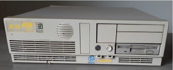
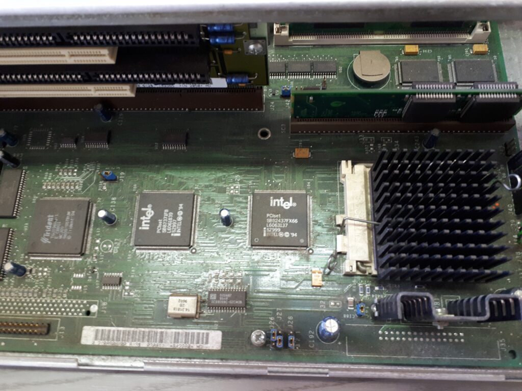
The Computer on display (Figure 19) is a much more recent version of the initial one and is based on a 100 MHz Pentium. This PC is contained in a 36x41x11 cm box. Figure 20 shows (part of) the motherboard.
4.2. Apple MacIntosh 512
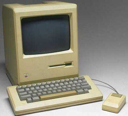
This computer was introduced in September 1984 and produced until April 1986. It represented the first update to the original MacIntosh 128 introduced in early 1984.
At the time of launch, its price was $2,795. It looked as in Figure 21. It had a driver for 3.5 diskettes that had to be inserted into the opening under the screen; no hard drive was provided. The video was 9″ B&W, with a resolution of 512×342 pixels. The measurements were 35x24x28 (HLD); it weighed 7.5 kg. At introduction, version 1.1 of the MacOS operating system was pre-installed; Before its retirement, the Mac 512 had reached version 4.1 of MacOS.
4.2.1. Motherboard of the MacIntosh 512
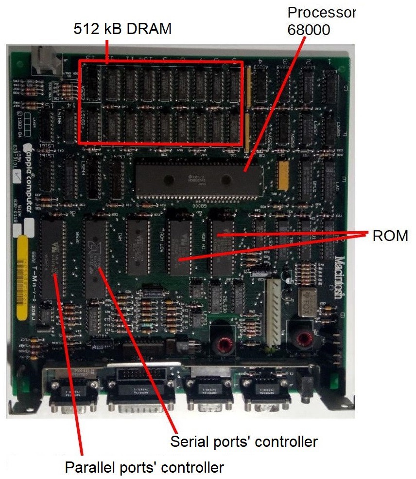
The motherboard, shown in Figure 22, was mounted horizontally under the floppy disk driver. The 4 connectors (female) that can be seen in Figure 22 protruded on the back. Orderly, from left to right, they represent these 4 doors: mouse port (9 pin), proprietary parallel port (19 pins) for a possible external floppy disk, serial port 422 (9 pins) for a printer, serial port 422 (9 pins) for a modem.
These were the main characteristics of the motherboard: the processor was a Motorola 68000 (in this specific case it is a Hitachi, produced under Motorola license), at 8 MHz (to be precise 7.8336 MHz); it had 512 kB memory, consisting of 16 integrated circuits of 256 Kx1bit, plus two integrated ones for parity control; ROM memory was 64 kB (two chips). In addition, there was a Z8530 serial port controller (produced by AMD under a Zilog license), and a VL6522 Parallel Port/Timer Controller (VLSI). Dimensions were 22×27 cm.
Between the serial port controller and the ROM, there is a custom VLSI integrated circuit. All the integrated circuits are soldered directly onto the board, except the two ROM integrated circuits, which are instead mounted on sockets. They contain (part of) the operating system. Evidently, there was a prediction that the content of the ROM could be subject to evolution.
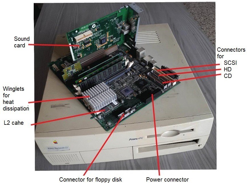
4.3. Apple Power Macintosh G3 M3979
This computer was introduced in November 1997 and produced until April 1998 (replaced by updated versions). At the time of introduction, its price was $2,400. Figure 23 shows the computer box with its motherboard on top of it. The following were the main features of the Power Macintosh G3 M3979. A PowerPC 750 microprocessor (page 20), operating at 233 MHz, mounted on a ZIF (Zero Insertion Force) socket; standard RAM 32 MB, expandable up to 192 MB; L1 Cache 64KB; L2 Cache 512KB (on 117 MHz bus); bus speed 66 MHz; cache bus speed 117 MHz; ROM/Firmware size 4 MB; Standard VRAM 2 MB, expandable up to 6 MB; 1024×768 pixel color display; 3.5″ hard disk, 4.0 GB capacity, IDE/ATA-2 interface optical disk; floppy disk. It had also a SCSI interface for external and internal additional disks. There were a 10Base-T Ethernet port and 3 PCI (Peripheral Component Interface) slots at 33 MHz. The operating system was MacOS 8.0. Motherboard dimensions: 28×20.5 cm.; dimensions of the case: 6.3 x 14.4 x 16.9 cm; weight approx. 10 kg.
Apple stopped making machines with G3 processors in October 2003.
Excluding the small machines of the debut, in which the 8-bit 6502 microprocessor was used, Apple initially used the 68000 processors (Motorola); between 1994 and 1996 it switched to PowerPC; between 2005 and 2006 it switched to Intel processors. Recently, Apple has also abandoned Intel processors switching to in-house production [6], [7].
4.3.1. Power Macintosh G3 M3979 motherboard
Figure 24 shows further details of the motherboard on display.
The processor and cooling winglets have been disassembled to reveal the socket on which the processor is mounted.
The DRAM memory consists of 3 modules of 32 MB for a total of 96 MB. A module has been disassembled and photographed on the right of the motherboard. The DRAM modules are all DIMMs (Dual In-line Memory Modules). The disassembled one and that appearing at the center of the photo have 16 integrated 2 MB. The third module (the left- most memory card seen vertically) instead is made of 8 ICs by 4 MB. modules. The system ROM is photographed to the right of the removed DRAM module; it is a SIMM (Single In-line Memory Module) that carries 2 ROM ICs by MB. The card features two integrated 128K 32-bit Video RAMs.
The SCSI port is for external SCSI disks (additionally, a SCSI connector is also provided for mounting disks inside the box). The system is equipped with an Audio card (Figure 23), which is mounted on the connector for personality cards.
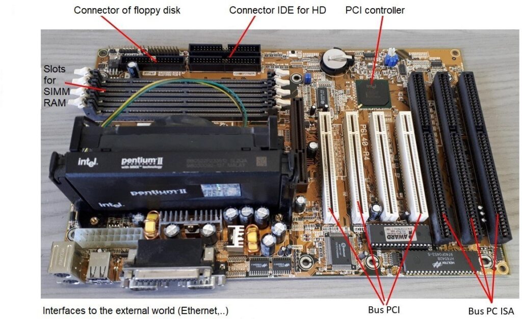
4.4. Desktop PC motherboard with Pentium II
This card was produced in 1999. It is interesting because it belongs to the era in which some new standards began to establish themselves while some old standards held. Apart from the Pentium II, the card features 3 connectors for the traditional PC ISA (Industry Standard Architecture); 4 PCI connectors; 2 IDE (PATA) hard drive connectors; 1 connector for Floppy disk; Dimensions: 30×19 cm.
On the board, the integrated circuit that acts as a PCI controller (Intel FW 82371AB PCI set) can be seen. The processor hides the RAM controller (Intel Fw82443lx Pentium Dram Controller). Behind the processor, there are 4 connectors for SIMM memory modules.
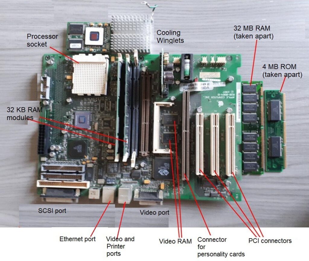
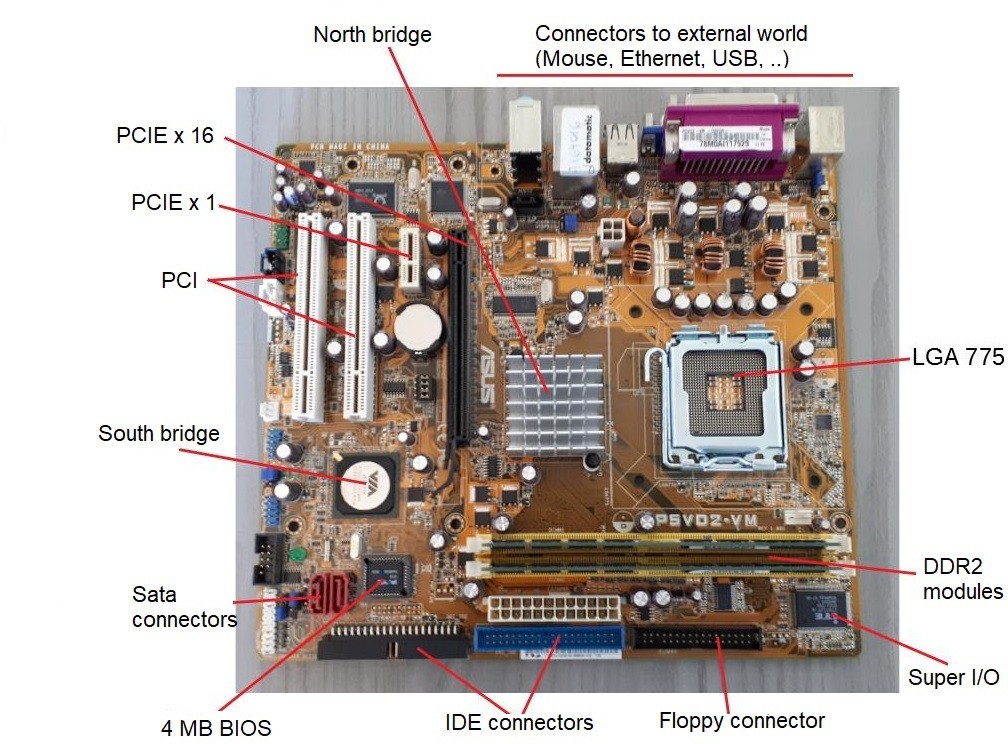
4.5. Motherboard ASUS P5D2-VM with Pentium Dual Core E2140
This board was produced for a few years starting in 2006. It has an LGA 775 socket on which Core 2 Duo, Pentium D, Pentium 4, and Celeron D processors can be mounted. In the specific case of Figure 26 the board featured the Pentium Dual Core E2140 (described on page 20). The board carries two 1 GB DDR2 DIMMs.
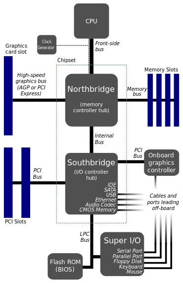
To illustrate the organization of this system let us refer to the scheme of Figure 27.
This organization was essentially introduced with the Pentium and was also adopted for the class of processors like the Core 2 Duo. It is no longer used for more modern microprocessors, for which serial buses, such as QPI, are in use. From the CPU the so-called Front-Side Bus (FSB) comes out connected to the so-called Northbridge. This creates the AGP bus (graphics) or the PCI express bus, plus the bus to the memory. The Northbridge is connected to the Southbridge which in turn creates a series of (relatively) low- speed buses, i.e. the external buses (IDE, SATA, Ethernet, USB, ..), the PCI bus, plus the traditional PC bus. The BIOS ROM is connected to the Southbridge, as well as traditional low-speed buses (parallel port, serial port, keyboard, mouse, ..). Note that in this way, the BIOS can sit on ROM memory which is seen exactly as in the original PC. (Northbridge and Southbridge form the so-called Chipset.)
4.6. Motherboard of the “SuperServer” 6013A-T
The SuperServer 6013A-T was produced around 2005 by the company Super Micro Computers. The system had the classic blade shape for rack mounting. Dimensions 4.3 x 42.6 x 57.4 cm (HLD); weight 15.9 kg. Figure 28 shows a blade.
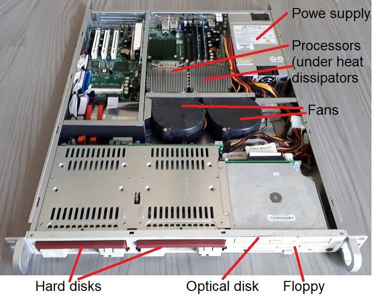
A blade was a dual-processor server. Figure 29 presents the main elements of the system. Observe the two fans, whose purpose is to force the circulation of air between the cooling winglets of the processors. Up to two hard drives can be mounted (SATA) hot swap. There is an optical disc drive and a floppy disk. The motherboard (X5DPA-TGM+) occupies approximately half of the horizontal surface of the blade.
Figure 29 shows both the image of the card and the diagram of the layout of the components. The meaning of some components is illustrated below. There are two sockets on the board for mounting Xeon processors. In the picture one of the sockets is empty, while the processor is mounted on the other, hidden by the winglets of the heat sink. In the specific case of the board shown, two Xeon 2800dp/512/533 were mounted.
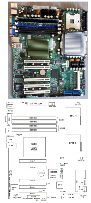
In summary, the main features of the motherboard were as follows: up to 2 Xeon processors (usable with socket 604), with frequencies up to 3.2 GHz; up to 8 GB of memory (using 4 x 2 GB DIMMs); two SATA ports for connecting two RAID disks (the ones on the front of Figure 28), hot-swappable; blade dimension was 30×25 cm.
4.7. SPARCstation 1
The SPARCstation 1, aka the Sun 4/60, was the first SPARC- station, sold by Sun Microsystems. It was marketed in April 1989, production ended in 1995. The SPARCstation 1 represented Sun’s fourth computer model using SPARC processors. The box containing the electronics (Fig. 30), due to its very flattened shape, was defined as pizza box.
SPARC stands for Scalable Processor ARChitecture, a RISC architecture defined by Sun Microsystem in the early eighties. The SPARCstation 1 sold for around $9,000 in the version without the hard drive, up to $20,000 in the most extended version. The motherboard (Figure 31) has connectors for the Sbus, the bus adopted by Sun in its systems, one Ethernet port and one for SCSI bus (at 5 MB/s). The Sbus remained in vogue for years, until it was supplanted by PCI and PCIe even on Sun machines. From the photo the processor is not visible, nor the arithmetic coprocessor Weitek 3167 coupled to it, as they lay under the card of video control logic.
5. Electronic memories
The exhibit contains a magnetic core memory, some integrated ROMs and EPROMs, a couple of memory expansion cards, and several modern memory modules for PCs or Servers.
Below we describe the magnetic core memory, the HP and Multibus expansion cards, two more recent memory cards, plus a cache expansion.
5.1. A core module
Core memory was developed at MIT in 1951 [8] and has been used as random access memory (RAM) from the mid-1950s to the mid-’70s. It became obsolete when semiconductor RAM became available at a convenient price.
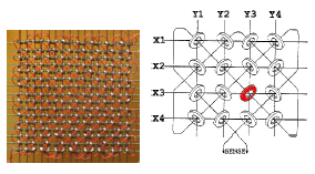
Figure 32 shows the core memory in the exhibit. The nameplate shows the diction “Memoria C.B.N. 16x8x7”, indicating that it is organized as a three-dimensional matrix of 18x8x7 bits. It was part of an Olivetti computer, presumably an Elea [9]. Apparently, the module was built by Olivetti with Mullard material. The latter was an English company that produced vacuum tubes (valves) and iron cores.
The organization of the memory module of Figure 32 is somewhat unusual. Normally, core memories were formed by a matrix of magnetic cores in a toroidal shape, as shown in Figure 33. Each nucleus had the function of a single bit and it was crossed by three wires, as per the diagram of Figure 33. The nuclei were arranged with their axis parallel to the plane and inclined by 45°, in such a way as to make the passage of the three wires. Referring to the diagram, the single ring is addressed via a pair of lines (X, Y), while the third wire (SENSE) serves as a reading and inhibition line. The operation is based on the hysteresis of ferromagnetic materials: a core subjected to an adequate magnetic field tends to maintain its state as long as another magnetic field does not reverse it.
To bring a nucleus to 1 it was necessary to make a flow of current through the relative X and Y wires. The value of the current was such that it affected only the nucleus at the intersection, while all the other nuclei on X and Y did not change the state.
The reading mechanism was quite complex. It began writing a 0: if the addressed core contained 1, a pulse appeared on the SENSE wire, due to the change in polarization of the nucleus; if instead, the bit contained 0 the pulse did not appear. Note that this technique is destructive of the nucleus content since its status is always brought to 0, therefore a subsequent write was necessary to bring back the state to 1, if that was the previous state. But if the state of the core had to remain at 0 it was necessary to inhibit the writing. In the first versions of these memories there was a specific Inhibition wire. Later, the SENSE wire was used (since the recognition function was not used while writing), to issue a current that generated a field opposite to that of the pair (X, Y), leaving the nucleus at 0. The controller of the memory had to switch the function of the line depending on whether it was reading or writing.
Referring to parallelism, if, for example, a parallelism of 8 bits was to be implemented, 8 matrices (planes) of nuclei were required.
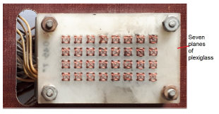
The 16x8x7 memory module is organized on 7 floors. Looking at the device closely (Figure 34, or, better, the lower image of Figure 32), 7 planes of plexiglass are seen. On each plane, there are 16×8 small holes (Figure 34), each of which is crossed by 4 wires. It can be deduced that the magnetic cores are placed and embedded in the plexiglass, with the hole of the ring corresponding to the small holes in the plexiglass, as to be crossed by the 4 wires; it can also be deduced that both the SENSE and the Inhibition lines were present.
On the front of the module (lower image in Figure 32 there is an array of female plugs. This suggests that the address lines and the two SENSE and Inhibition lines were brought to the module through pins or through a matrix of pins on which the front panel was fitted.
Note: Elea is the name of a series of computers developed by Olivetti in the second half of the fifties. The term “Elea” was chosen regarding to the colony of Elea in Magna Greece, home of the Eleatic school of philosophy (Parmedine, Zeno of Elea). The Elea 9003 was announced in 1959; the first example was delivered in September 1960. According to Olivetti publications, the Elea 9003 was the first commercial computer in the world entirely made with solid-state components (transistors). However, this statement can be hardly shared; exist, in fact, photos advertising IBM’s 7070, introduced in 1958, the first computer using only Transistor.
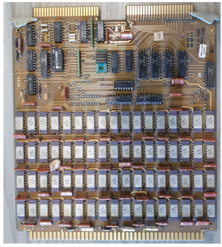
5.2. 16 kB 16-bit word memory expansion card for HP 2100 computer
The expansion card in Figure 35 was mounted on the internal (proprietary) bus of the HP2100 minicomputer. The contacts towards the bus are the ones at the bottom. The dimensions of the card are approximately 19×20 cm. It uses the 4027 memory chip, containing 4K x 1 bit. On the card, 4 rows of 17 chips can be seen; they give rise to 16K 16-bit words. The seventeenth serves for parity control on each row. The HP 2100 minicomputer was introduced in 1971 and was the first of the HP2xxx series to be equipped with electronic memory (dynamic RAM). The previous models, HP 2116 and HP 2115, introduced in 1996 and 1997 respectively, used magnetic core memories.
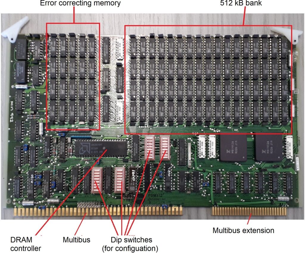
5.3. 5 MByte Memory Expansion Card for Multibus
This board was produced by the English company Plessey in the early 1980s (Figure 36). It was designed to be mounted on the Multibus. This bus, defined by Intel, was very popular from the late 1970s through the 1980s. It was standardized by IEEE as the IEEE 796 bus. In 1982 there were over 100 industries producing cards for the Multibus. The board uses M3764 memory ICs, 64K x 1-bit dynamic RAM, in a 16-pin DIP.
The matrix of 17 by 4 memory chips forms a 512 KB memory bank, plus parity (16x4x64K/8). The integrated 5 by-4 memory matrix serves for error detection and correction. The cycle time was 500 nanoseconds, with an access time of no more than 300 nanoseconds. There were 4 devices (Dip switches) to configure the operating mode of the board. In addition to addressing, they allowed the selection of 8 or 16-bit operating modes. This was typically derived from the fact that on the Multibus could be used cards with 8 or 16-bit CPUs, typically the 8088 or 8086. Also, note the AMD 2964 dynamic memory controller.
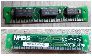
5.4. 256 kB Memory module
The part in figure 37 has been one of the first memory modules in a modern format. It was manufactured by MBS (Japanese) in the early 1990s and is marked as NMBS TCC- T-H7V. Capacity was limited to 256 kB. In the upper image, the two chips form a 256 kB block (their exact characteristics could not be traced); the third chip is presumably the memory controller, specially produced for those memory devices.
Note that the size of the plate is about 9 cm, and there is no notch. Subsequently, modern memory modules have been standardized, first with SIMMs and DIMMs. These have a size of less than 11 cm and a notch for their correct placement.
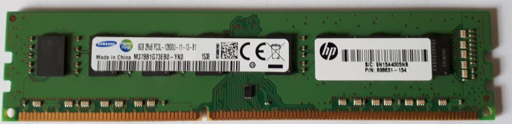
5.5. 8GB DIMM Memory module, DDR3 (Samsung M378B1G73EB0-YK0)
The DIMM M378B1G73EB0-YK0 (Figure 38) features 16 Sam- sung K4B4G0846E 4 Gbit DDR3 memory chips, 800 MHz operating frequency, 1.35 V supply voltage. The nameplate says 8GB 2Rx8 PC3L-12800U. The transfer rate is 12.8 GB/s. Currently, this is the highest integration density memory module among those on display. The module was used on an HP laptop. It does not have the extra bits for error checking.
Note the notch.
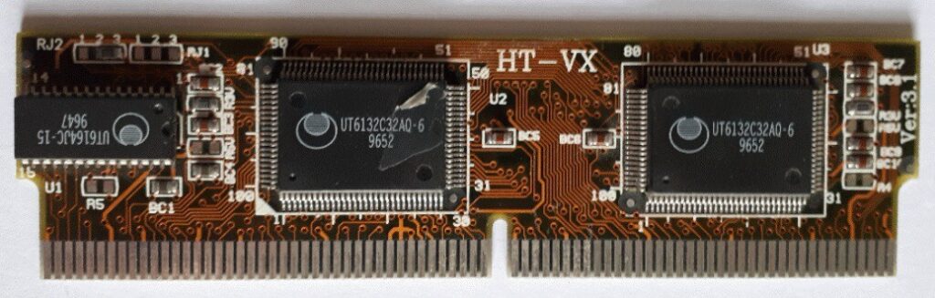
5.6. 256 KB cache memory module
The part in Figure 39 is a DIMM module (160 pins) functioning as a 256KB second-level cache memory. It is not known which system it came from (probably from a system based on the micro 80486). The production is Chinese. The ICs were produced by the no longer active Utron Technology company (production in Taiwan). The two UT6132C32AQ ICs (on the right in Figure 39) are synchronous SRAM (CMOS), organized as 32K 32-bit words. The UT6164JC integrated circuit (on the left) is instead a 32K byte SRAM (CMOS).
Presumably, it is a direct mapping cache organized as follows: the two integrated 32K x 32bit ones give rise to a data RAM of 32K by 8 bytes (i.e. 256KB of data RAM), while the third IC (32KB, equal size of the data RAM) is used to contain the Tags.
6. Storage Media
The exhibit contains storage media from the past such as punched cards, punched tapes, floppy disks, magnetic tape cassettes, and several hard disks. The following describes punched cards and tapes, flexible disk drives, and several hard disk drives.
6.1. Punched cards
Until the 1970s, punched cards were perhaps the main sup- port for programs and data. All computer centers were equipped with card readers and punchers. The format card standard was the one defined by IBM in 1928: 80 columns by 12 rows, on a cardboard measuring 1187.325×82.55 mm. One character could be encoded on each column through drilling. The cut corner, at the top left, was introduced to avoid possible errors regarding the position of the cards (on puncher or reader). Punched cards have had a long history. In 1801 Joseph Jacquard used cardboard punched cards for controlling a weaving loom that became known as a Jacquard loom. In 1837 Charles Babbage, the creator of the first programmable computer, adopted Jacquard’s punched cards for controlling the sequence of computation for his analytical machine; it was still a mechanical machine. In 1885 Herman Hollerith used his tabulating machine to read and count data punched on index cards to take a census of the population of the United States. The company founded by Hollerith in 1896 Hollerith, the Tabulating Machine Company, through some steps, became IBM (International Business Machines) in 1924).
Examples of cards are pictured together with floppy disks in Figure 41.
6.2. Punche tape
Until the 1970s, while traditional computer centers used punchers and card readers, minicomputers were equipped with punchers and tape readers. The tape was made of paper or plastic material (Mylar).
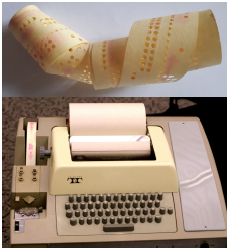
The reader was normally of the optical type. Even teleprinters, often used as consoles, could be equipped with a tape reader/puncher. Figure 40 shows one of these ma- chines (a Teletype). Note that the tape reader/puncher is part of the teleprinter. A piece of punched tape is shown above the teleprinter. On the tape, each character was punched across 8 bits, usually in ASCII coding for alphanumeric characters, or directly in binary. Note that in addition to the 8 (possible) holes for the character, a much smaller hole was also produced in correspondence with each of them. This was to give synchronization. In the case of optical readers, the tape was pulled by a conveyor; the little hole gave the synchronization to read the 8 bits at the right time, providing a time window centered on the character’s transit window. The striping of the little holes divided the characters into 3 and 5 bits.
6.3. Floppy disks
Flexible (floppy) disks were the inevitable elements in any kind of system until the first five years of the 21st century. Subsequently, they began to disappear, replaced by memory sticks.
In 1967 IBM began studying the development of floppy disks. In 1971, IBM also released the first floppy disk, in an 8-inch format, to transferring the microcode (i.e. the microprogram that gave rise to the hardware behavior of the machine) into the control memory of the System/360. Shortly thereafter, the IBM employee responsible for the project (Alan Shugart) founded his own company to produce 8” floppies. This format was abandoned in 1976 in favor of the 5.25” format. In both of these, formats the container was a plastic bag. Subsequently, the industries began to produce disks with rigid cartridges measuring around 3″; but it was only in 1981 that Sony introduced the 3.5″ disk in the shape and structure that later became standard. Figure 41 shows an example for each of the three formats. The photo also shows some punched cards and a miniature CD.
3.5″ flexible disks
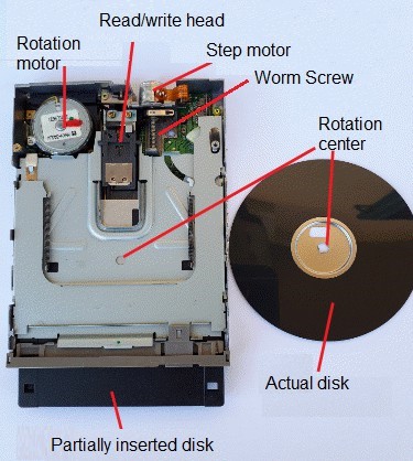
Figure 42 presents the details of the 3.5” floppy driver on display.
Next to the driver, there is the actual “disk”, deprived of its container. It is a disk of plastic material, Mylar, on which the magnetic layer that acts as an information sup- port is deposited. Note that a disk is partially inserted in the driver, and the metal part still covers the window on which the reading/writing head moves. The metal cover is automatically moved when the disk is completely inserted, to allow the head to face the actual disk.
When inserted, the disk is kept in continuous rotation, driven by a transmission belt guided by the rotation motor; the belt follows a non-direct path between the motor and the rotating element. The read/write head is driven by a step motor. Looking at the image of Figure 42 a worm screw in the axis with the step motor is seen. This screw engages with the head and causes it to move forward/backward (in the vertical direction in the image).
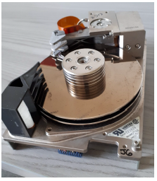
6.4. Hard Disks
Until recent years hard disks have been the most important auxiliary storage devices. Currently, SSDs (Solid-State Drives) tend to replace them. The relatively low cost per byte and the non-volatility of the information stored in hard disks make them suitable for long-term storage. The following description refers to modern hard drives, i.e. disks contained in a sealed cartridge. The first version of these disks was introduced by IBM in 1973. The drive was, in reality, made up of a fixed part and a removable part, both 30 MB. The device was called “Winchester 30-30” from the name of a rifle, the Winchester 30-30, owned by one of its designers, and thus the related technology was called Winchester technology, but this term disappeared since all hard drives are now in sealed cartridges.
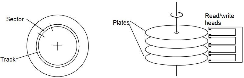
The diagram in Figure 43 shows that a modern hard disk is made up of a certain number of plates (aluminum) whose surfaces are covered with a layer of magnetic material which acts as a storage medium. The diameter of the plates ranges from 1 to 5.25 inches. 3.5″ disks are normally used in desktop computers and server systems; 2.5″ are used in laptops. The plates are in constant rotation, with a constant speed normally included between 3600 and 15000 g/m. The read/write heads are integral to each other. The dishes and the read/write heads are inside a sealed, vacuum container. This requires extremely refined mechanics. Each magnetized face is subdivided in tracks, i.e. in concentric circles on which the data are stored. The number of tracks per face ranges from 1000 to 5000. Each track is divided into sectors. The number of sectors per track ranges from 64 to 200. For a given disk the number of sectors per track is constant, regardless of the diameter of the trace. As a result, there is a decreasing storage density from the center towards the periphery. The sector is the smallest read/write unit. Traditionally, the typical sector size is 512 bytes, but also larger sizes (1024, 2048 bytes) are in use. The average time required by the head to position itself on the addressed sector is called Average positioning time.
The most common hard drives present one of the following interfaces:
- ATA (Advanced Technology Attachment), introduced in 1986, for which they are also used other names (IDE, EIDE). Since it is a parallel interface today it is normally indicated as In 2003, the serial version of it, named SATA, has practically completely replaced PATA.
- SCSI (Small Computer System Interface), introduced in 1978 under the name SASI (Shugart Associates System Interface) from the name of the disk manufacturer who proposed it, became soon a very popular industry standard. The original SCSI was a parallel interface, designed to connect a high number of devices, not necessarily disks. Successively, the interface has undergone a significant number of updates. The serial version (SAS, Serial Attached SCSI) was introduced in 2003; it is also replacing the traditional parallel.
6.5. The Diablo 40 Series Hard Drive
As stated previously, before the emergence of modern sealed drives, hard disk drives included a fixed and a mobile disk. The dimensions of the plates were much larger than the current ones.
The image on the left of Figure 44 shows the platter of one of these disks. The diameter is 14”, or 35.56 cm. The platter was made of aluminum and covered with magnetic material. The moving plate was itself enclosed within a cartridge which could be removed and replaced with another cartridge. Given its size and shape, the removable cartridge was called (at least in Italy) frying pan.
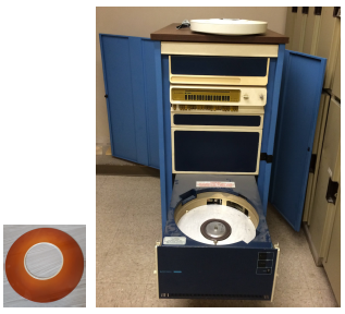
The image on the right of Figure 44 shows one of the most successful minicomputers of the seventies: the Data General Nova 3, introduced in 1976. A cartridge rests on the top shelf of the rack. The lower part of the image shows the compartment where the cartridge had to be inserted.
This hard disk belonged to the Series 40 Diablo. Diablo was a sub-brand of Xerox, and these disks were widely used with minicomputers up to the seventies. They had a capacity of 5+5 MB (5 fixed and 5 mobile). Interchangeability potentially allowed an unlimited disk space.
Data General was founded in 1968 by leavers from Digital Equipment Corporation (DEC), including Edson de Castro, the designer of the first commercial minicomputer in history the Digital’s PDP-8. Both Digital and Data General are long gone. Digital was purchased in 1998 by Compaq, which was later merged into Hewlett-Packard in 2002; Data General was purchased in 1999 by EMC, which later became Dell.
6.6. Vertex V130
The platters of the Vertex V130 had a diameter of 5.25″, a format that is now abandoned. The hard drive in question (Figure 45) was part of an HP9000 station; these were his characteristics: 5.25 inch format; capacity 26 MB; number of sectors 50,337; Bytes per sector 512; average positioning time (seek time) 30 ms; transfer rate (max) 0.625 MB/S; rotation speed 3600 rpm; number of disks 2; number of read/write heads 3; production period early 1980s.
6.7. IBM DSAA-3540
The disk in Figure 46 was part of a series called Dekstar produced by IBM. The series was introduced in 1994 by IBM, passed to Hitachi at the end of 2003, and then to Western Digital which abandoned its production in 2018. The DSAA 3540 model is from the second half of the first decade of the 2000s.
These were the main features: size 3.5″; capacity 527 GB; IDE-AT interface; 12.0 ms average positioning time (seek time); 1,240 cylinders; 63 sectors per track; 512 bytes per sector; 8.3 MB/s transfer speed; 4,500 rpm rotation speed; 2 plates; 3 read/write heads (the central head operates on two faces); weight 530g.
6.8. Quantum Fireball Plus LM
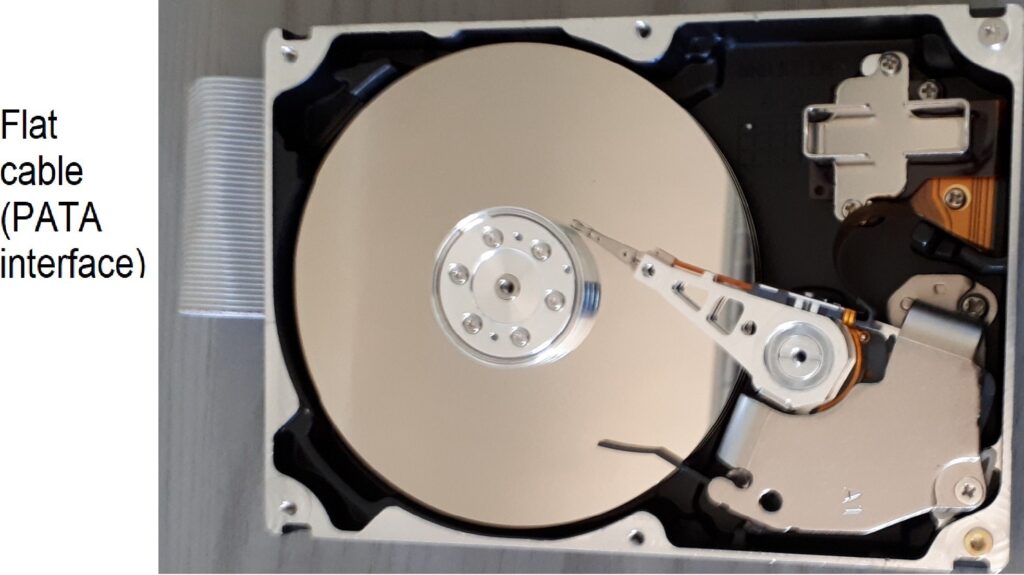
Figure 47 shows the Quantum Fireball Plus LM. It was introduced in 2000, and manufactured by Quantum Corporation. These were the main characteristics: size 3.5″; capacity 20.5 GB; interface type ATA-66; average head positioning time (seek time) 8.5 ms; transfer speed 66 MB/s; rotation speed 7,200 rpm; number of plates 3; number of read/write heads 6.
Please note the connection cable for the PATA interface (flat cable on the left side). Compare this cable with the SATA cable in Figure 48.
6.9. Seagate Barracuda 10 Modello ST 3250310 AS
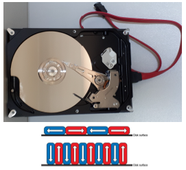
The Barracuda 7200.10 series (from Seagate Technology) includes drives ranging from 80GB to 720 GB. Both 1.5 Gb/s or 3 Gb/s SATA interfaces and a PATA 100 interface, are available for them. This series was introduced around 2006. The main characteristics of the specimen in the show are as follows: size 3.5″; capacity 250 GB; SATA type interface; average rotation latency time 4.16 ms; average transfer speed 125 MB/s; rotation speed 7,200 rpm; number of plates 2; number of read/write heads 3.
The SATA connection cable was left on the specimen of Figure 48. Compare this cable with the PATA cable of the Quantum Fireball Plus of Figure 47).
It is worth noting that, to increase storage density, this disk adopts vertical storage, differing from previous products where the bit orientation was horizontal (refer to Figure 48).
7. Microprocessors
In November 1971 in a then very widespread electronics magazine (Electronic News), this ad appeared: Announcing a new era of integrated electronics. A micro-programmable computer on a chip! Since then the term “microprocessor” has been part of the common lexicon.
The exhibit contains a substantial number of microprocessors, largely belonging to the x86 family. There is also a precursor of microprocessors technology, that is SLT logic and we start describing it.
7.1. Solid Logic Technology
The Solid Logic Technology (SLT) was the precursor to integrated circuits in the form we know today. It was introduced in 1964 by IBM in System/360. It represented the first example for miniaturized semiconductor circuits of large industrial production (Figure 49).
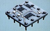
SLT devices were denser and faster than devices using separate transistors and consumed less energy. These were hybrid circuits, including transistors and diodes, mounted on a ceramic base having a surface area of half an inch square, as illustrated in Figure 49. Figure 50 shows one such component.
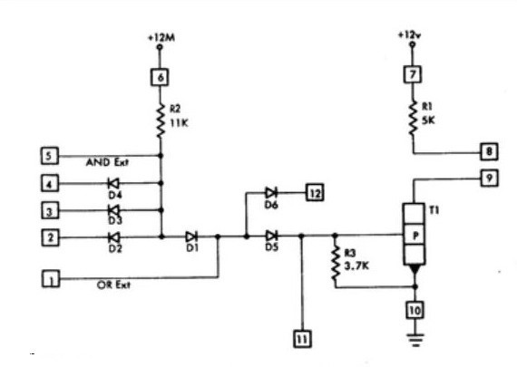
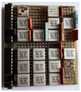
Figure 51 shows an SLT module used in the S/360 system. Various components appear mounted on the module; four of them correspond to the mentioned IBM component 361493.
7.2. The 8008 microprocessor
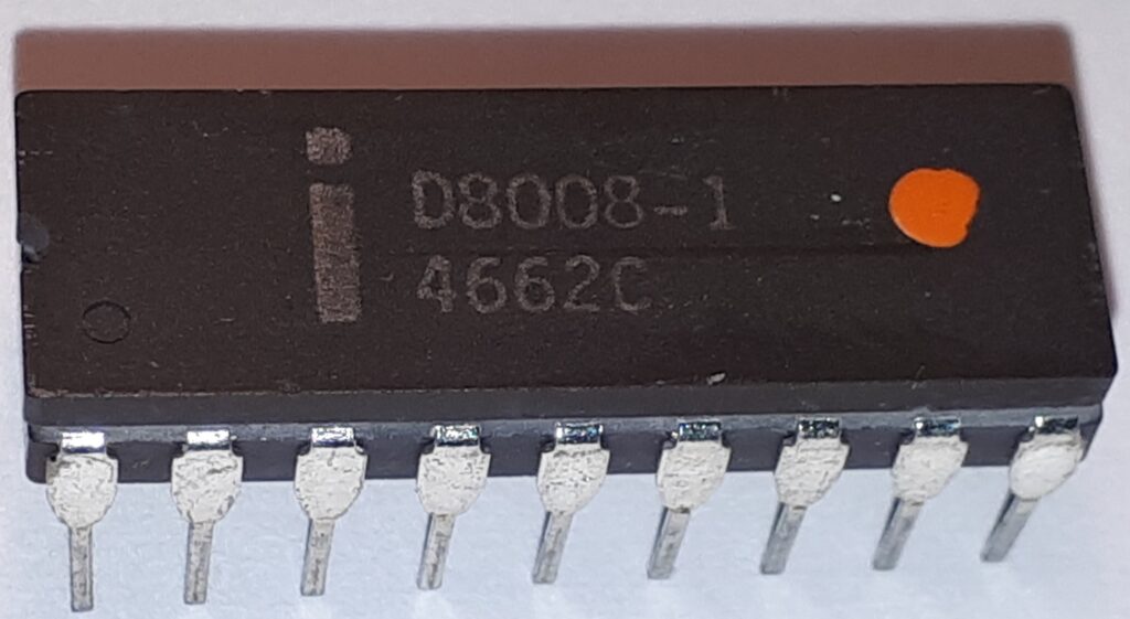
The 8008 (Figure 52) was produced by Intel and released in April 1972, just over a year after the first microprocessor, the Intel 4004 [2], produced with the fundamental contribution of Federico Faggin [3].
These were the main characteristics 8008: 0.2 MHz clock frequency, 3,500 transistors in an 18-pin DIP package. The address space was 16 kB (14-bit address lines). There was a single 8-bit bus (for data and addresses); as a result, to access memory, several clock cycles were required. In fact, it was necessary to present the 14 address bits in two successive phases, so that the address could be captured on an external latch (first 8 bits and then the remaining 6); the data (8 bits) passed on subsequent machine cycles.
A detailed description of the 8008, as well as of the 8080, 8085, and 8086 can be found in [10].
Note that the 8008 was commissioned by the Data- point company, aiming at its use in the Datapoint 2200 programmable terminal. However, the device was delivered too late and did not meet the client’s expectations in terms of performance. It was therefore not used in the Datapoint 2200.
7.3. The 8085 microprocessor
This was an 8-bit microprocessor introduced by Intel in 1976; production continued until 1990. These were its main characteristics: clock frequency 3.5 MHz; 6,500 transistors in a 40-pin DIP package; address space 64 KB; 8-bit data bus, 16-bit address bus. The data bus is multiplexed with the lower part of the addresses.
The 8085 was the improved version of the 8080, a highly successful 8-bit processor, introduced in 1974. Specifically, the 8080 was the first widely used microprocessor, used not only to replace wired logic but also for the creation of personal computers (then called microcomputers), being able to address a memory space 64 kB of memory space, which was considered even excessive at the time. The instruction set of the 8080 was significantly influenced by that of the 8008.
The 8085 had a single supply voltage of 5V, hence the “5” as the last digit in its name. Whereas, the 8080 required two additional supply voltages, -5V and 12V. Furthermore, the 8085 had a more refined interrupt system than that of the 8080. In its use in personal computers, the 8085 and 8080 were outclassed by the Z80.
7.4. The Z80 microprocessor
The Z80 was introduced in 1976. It was designed and developed by Zilog, a company founded by F. Faggin, after he left Intel. These were its features: clock frequency 2.5 MHz; 8,500 transistors in a 40-pin DIP package; 4-micron MOS technology; 64 KB address space; 8-bit data bus, 16-bit address bus, distinct; It had a compatible but more extensive repertoire of instructions than that of the 8008/85 and had a more advanced I/O management system.
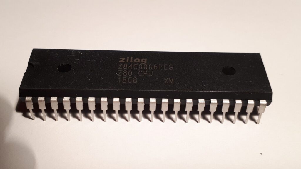
The Z80 became very popular in the construction of personal computers. At the time, the dominant operating system (also working on 8080/85) was CP/M, which was swept away by the arrival of PC-DOS for 8088.
The Z80 was produced by a large number of electronics companies, including Hitachi, SGS-Thomson, NEC, Sharp, Toshiba, National Semiconductor, and Mostek. It is still produced today. Furthermore, there are various SoCs (System on a Chip) in circulation that incorporate the Z80, as well as various IP (Intellectual Property) core containing the Z80. IP cores are designs or specifications of logic that are licensed to build devices; they are typically used as building blocks for ASIC (Application-Specific Integrated Circuit) circuits.
7.5. CDP 1802 microprocessor
This microprocessor (Figure 54) was introduced by RCA (Radio Corporation of America) in 1976. RCA has been one of the most important American companies in the field of electronics. Currently the RCA brand belongs to a French multinational.
Originally the CDP 1802 was designed for use in personal computers (home computers), but, irony of history, due to its peculiar characteristics (low consumption and static logic) it found great use in embedded applications.
The address bus was 8 bit-wide, therefore the 16 bits of the bus were transmitted on two successive clock cycles.
The two characteristic aspects that differentiated the CDP 1802 from the microprocessors of the time, normally in nMOS or MOS technology, were the CMOS technology and the static logic. The CMOS technology led to reduced consumption, while the static logic allowed the clock frequency to be brought to zero; in this case, the processor maintained its state as if it were in a halt state, but without the consumption corresponding to the dynamics imposed by the clock. For this reason, it had some success in space applications, as static logic was considered more resistant to radiation. A radiation hardened version was also built, specifically for space missions.
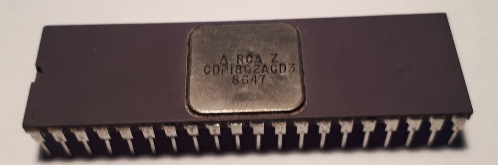
The CDP 1802 (also known as COSMAC, from the name RCA gave its CMOS process: complementary silicon/metal- oxide semiconductor) was used in the Galileo mission. The spacecraft was launched in October 1989 and reached Jupiter in December 1995; orbited the largest planet in the solar system for almost 8 years. Out of curiosity, we report the dimensions of the software: 650,000 lines of code for orbital control, 1,615,000 lines for telemetry, and 550,000 lines for navigation. Obviously, the spacecraft had a multitude of microprocessors.
The example on display (Figure 54) is the model CDP 1802ACD3, an improved version of the initial 1802.
7.6. The 8086 microprocessor
The 8086 [10] represented a milestone in the development of computing. It was Intel’s first 16-bit microprocessor and defined an architecture that is still referred to as “x86”. Almost any personal computer contains a processor whose roots lie in the distant progenitor 8086. The use of x86 architecture processors is not limited to personal computers: they are the basis of many server systems and many supercomputers.
Over the years, the original 16-bit version was extended to 32 and later to 64-bit. The 64-bit extension, with which segmentation was practically put aside, was defined by AMD – not by Intel. Given the great popularity of the x86 architecture and the great acceptance of its extension to 64 bits, the giant Intel was somehow forced to adopt it, abandoning other projects for 64-bit machines. Intel continues to be the largest manufacturer of x86 processors, followed, at some distance in terms of numbers, by AMD.
The 8086 was introduced in June 1978. These were the features of the introduction model: Clock frequency of 5 MHz; 29,000 transistors in a 40-pin DIP package; 1 MB address space; 16-bit data bus, 20-bit address bus data and address bus multiplexed.
The state of technology of the time, the constraints imposed on the design (presumed compatibility with the 8085 8-bit microprocessor, and use of a 40-pin integrated circuit), and the intent to define a sophisticated protection system had a notable influence in determining the architecture and making it a little complicated; specifically, the 8086 featured a segmented memory model, a model that was substantially put aside by the 64-bit architecture. The limited number of pins also imposed multiplexing of the data and address bus.
The average number of Clock cycles Per Instruction (CPI) could be estimated at 15. Thus, at a clock rate of 5 MHz, the average time to execute an instruction is 15 ∗ 200ns = 3µs , corresponding to a performance level of approximately 0.33 MIPS (Million Instructions Per Second).
The 8088 microprocessor
The 8088 (Figure 55) is the 8-bit version of the 8086. It was introduced about a year after the 8086. The 8088 is a CPU completely compatible with the 8086: it has essentially the same internal structure, like the 8086 it has a memory space of 1 MB, but has an 8-bit external data bus.
In 1981 IBM introduced a personal computer, the IBM PC, based on the micro 8088, with a clock frequency of 4.77MHz. The choice of the 8088 essentially arose from cost reasons: the 8-bit data bus made it possible to reduce the costs of the electronics compared to those of an equivalent 8086-based system. Moreover, at the time the peripherals that could be used on Personal Computers (PCs) were practically only 8-bit, while the speed of the 8088 (although lower than that of the 8086) was even excessive for the typical applications of the time.
The IBM PC was not the first personal computer to make its appearance on the market. For years, a variety of personal computers based on 8-bit microprocessors such as the 8085 and the Z80 (all these kinds of machines had an address space limited to 64 kB) had been on the market. To get an idea of why the IBM PC enjoyed a huge favor, we must keep in mind that, until the beginning of the eighties, in the USA, which practically represented the computer market almost exclusively, the acronym “IBM” and the word “computers” were practically synonymous. When IBM introduced the PC, to the general American public it was as if the PC was born at that moment. Large users, such as banks, industries, state apparatus, etc., who had until then been refractory to the use of PCs, found their use completely natural, also by the supposed possibility of integration with existing IBM mainframes.
Time magazine, which traditionally dedicates the cover of the last issue of each year to the most distinguished person of the year, in 1981, to the surprise of its readers, dedicated the cover to the PC instead of to a person.
The adoption of the 8088 in the IBM PC and the success of the latter determined the success of the x86 architecture.
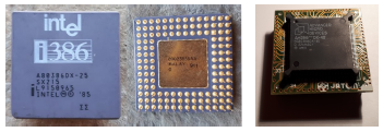
7.7. The 80386 microprocessor
The 80386 was the first 32-bit x86 architecture microprocessor 1. It is usually indicated as 386. Produced from October 1985 to September 2007.
These were the characteristics at the time of introduction: clock frequency 12.5 MHz; 275,000 transistors in a 132-pin Pin Grid Array (PGA) package; IA-32 architecture (x86 extension); separate data bus and address bus, both 32-bit.
In addition to doubled parallelism, the 386 introduced virtual memory paging after segmentation. The maximum virtual space was up to 64 TB. The 32-bit address bus allows a maximum physical addressing of 4 GB (compared to 64 TB virtual).
The 386 represented a milestone in the development of the x86 family, implementing the transition to 32-bit architecture. The 386 redefined the format of the instructions and extended the repertoire of the 8086 (for example by making the registers substantially interchangeable with each other, unlike the 8086 where they were instead specialized and therefore subject to a more limited use). The 386 did not yet have an integrated cache or floating point arithmetic. For the cache, the manufacturer made some ICs to build it externally; for floating point arithmetic, the 80387 coprocessor had to be used.
The photos in Figure 56 show two 386s on display: one Intel and one AMD. This second one is surface-mounted and is mounted on a socket to make it compatible with the Intel pinout.
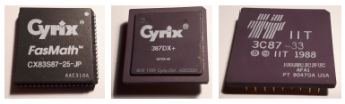
7.7.1. The 80387 coprocessor
A specific coprocessor was introduced for the 386, the 80387. Figure 57, shows three specimens on display.
7.8. The 80486 microprocessor
The 80486 (486 for short) was introduced by Intel in April 1989, production lasted until 2007. These were the characteristics at introduction time: clock frequency 25 MHz; 1 micron CMOS technology; approximately 1.2 million transistors into a 168-pin PGA.
With 486, a 5-stage pipeline was introduced: Prefetch (PF), Decoding (D1), Address Generation (D2), Execution (EX) and Write Back (WB). The creation of the pipeline required overcoming several problems related to the Complex Instruction Set Computer (CISC) structure of the instruction set.
The 486 was the first device of the x86 family to integrate the floating point unit (FPU) and a cache memory (8 kB) on the same chip. The actual acronym of the processor with FPU was 486DX. At the same frequency, the performance of the 486 was 2 or 3 times higher (depending on the type of processing) than the performance of the 386. With the 66 MHz DX2 version the performance of the 486 reached 54 MIPS.
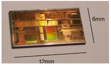
Figure 58 shows 486’s die on display.
In mid-1991 Intel introduced the lower-cost version of the 486, called the 486SX. It differed from the 486DX in that it lacked floating point (FPU) arithmetic. It is interesting to note that the first 486SX were substantially identical to the 486DX, i.e. they contained the FPU which, however, was disabled. The price was lower only for commercial reasons. Subsequently, towards the end of 1992, the FPU was removed to reduce production costs.
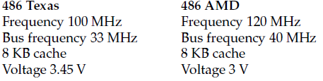
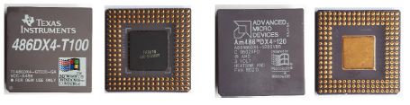
The 486 introduced a differentiation between the frequency of the processor and that of the external bus which, depending on the models, operated at a frequency equal to half or a third of that of the processor. On display, there are 2 examples of 486 (Figure 59), one produced by Texas Instruments and one produced by AMD (the pinout of these is also shown here, obviously identical). The dimensions are 4.45×4.45 cm. The second IC states that a heat sink and fan are required.
7.9. The Pentium microprocessor
The Pentium (Figure 60), introduced in March 1993, was the first microprocessor of the x86 family to cross the 100 MIPS threshold. These were the characteristics at the time of introduction: clock frequency 60 MHz; 3.1 million transistors, across 2.16 square inches, in a 273 PGA; 32-bit architecture.
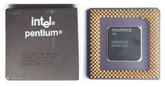
While maintaining software compatibility with previous models, the Pentium provided some additional instructions, including those that allow the implementation of the MESI (Modified, Exclusive, Shared, Invalid) protocol for cache coherence in multiprocessor environments.
The Pentium introduced significant innovations: 64-bit external data bus; superscalar architecture; pipelined floating point calculation; separate internal cache for instructions (8 kB) and data (8 kB); prediction of conditional jumps; speculative execution (limited to the presence of conditional jumps).
It is worth noting that with the Pentium, Intel abandoned the numerical denomination of its processors because numbers are not patentable and therefore any manufacturer could introduce a device and call it, for example, 386. The term Pentium was used to indicate that it was the successor to the 486. The Pentium acronym was used for many subsequent x86 models, until the adoption of the acronym “Core”.
7.10. Athlon 64 X2
This is the dual-core version of the Athlon 64 (this was the first 64 bit-processor of the x86 family). It has been produced from 2005 to 2009 by AMD (Figure 61).
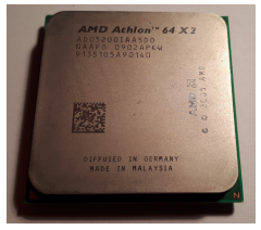
Main features of the processor are [12]: 64-bit architecture; operating frequency 2.7 GHz; 16 bit bus HyperTransport 1000 MHz (2 GT/s); FSB frequency 800 MHz; number of cores 2; 221 million transistors; 65 nm technology; two second-level caches of 512; compatible with Intel extensions MMX, SSE, SSE2, SSE3.
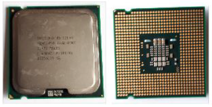
7.11. The Intel Pentium Dual Core E2140 microprocessor
The Pentium dual-core E2140 was introduced in 2007. The Pentium name was abandoned for this processor and is now referred to as Core 2 Duo. Main characteristics: 64-bit archi- tecture; operating frequency 1.6 GHz; bus frequency (FSB) 800 MHz; number of cores 2; 105 million transistors; 65 nm technology; 1 MB second-level cache; Land Grid Array (LGA) 775 type socket (i.e. with 775 possible contacts); extensions: MMX, SSE, SSE2, SSE3, SSSE3.
Despite having the name Pentium, this microprocessor, designed for desktop uses, adopts the Core microarchitecture, introduced by Intel in 2006. This microarchitecture is typically multicore and constitutes the continuation of the P6 microarchitecture, the one defined with the PentiumPro processor in 1995.
The example on display (Figure 62) was mounted on the ASUS P5D2-VM motherboard described on page 9 on which the LGA 775 socket can be seen. A heat sink and the related air movement fan were mounted on the microprocessor (see Figure 68).
7.12. The Core 2 Duo T5500 microprocessor
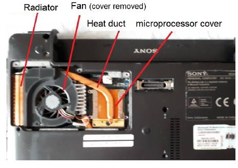
The Intel Core 2 Duo T5500 was introduced in 2008 for mobile computers. The example on display (Figure 63), was taken from a Vaio VGN-1GZ laptop computer (see Figure 69).
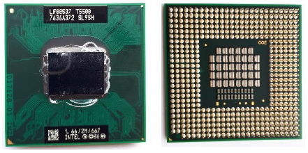
Main characteristics: 64-bit architecture; operating frequency 1.66 GHz; bus frequency (FSB) 667 MHz; number of cores 2; no hyperthreading; 291 million transistors; 65 nm technology; 2 MB second-level cache; socket PPGA478 (PPGA: Plastic Pin Grid Array; power supply 1,0375V-1,300V; extensions: MMX, SSE, SSE2, SSE3, SSSE3.
Main characteristics: 64-bit architecture; operating frequency 2.66 GHz; bus frequency (FSB) 133 MHz; number of cores 4; no hyperthreading; 473 million transistors; 45 nm technology; 6 MB second-level cache; socket 775; (PPGA: Plastic Pin Grid Array; power supply 0.8500V-1.3625V; ex- tensions: MMX, SSE, SSE2, SSE3, SSSE3.
7.13. The PowerPC 750 microprocessor
The PowerPC 750 was introduced in 1997 by IBM [13] and Motorola. It was one of the members of the 7xx family, also called the third generation (G3) of PowerPC processors, designed and produced by the AIM (Apple-IBM-Motorola) consortium, born in 1991 to define a new architectural standard, capable of counteracting Intel’s dominance. It was a RISC (Reduced Instruction Set Computer) architecture, based on IBM’s previous architecture called Power. When introduced, the PowerPC had the best ideas and implementation that could be put together.
7.14. The Core 2 Quad
The Intel Core 2 Quad was introduced in 2008. The example on display (Figure 64), was taken from an Asus PSQL PRO mother board.
At first, these CPUs were very favorably received by the market. Despite this, the PowerPC failed to counter the dominance of the x86 architecture, although it was used for a long time in Apple’s Macintosh (Figure 65). Since 2006, Apple has abandoned PowerPC processors in favor of Intel processors; more recently Apple has switched the entire Mac lineup to its own designed chips. IBM continued to produce PowerPCs and use them in various product lines (including some supercomputers).
The relevant features of the 750 model are as follows. Clock frequency at introduction 233 MHz; 6.35 million transistors, in a 360-pin CBGA (Ceramic Ball Grid Array) package; 64-bit data bus at 66 MHz; separate data and instruction caches of 32 kB each; dedicated 117 MHz external bus for a (unified) second-level cache.
Figure 66 shows the microprocessor and a module that mounts it together with a second-level cache memory.
Apple used the 750 model in the Power Macintosh G3, specifically in the M3979 model, described on page 7
8. Other elements on the exhibit
The exhibit contains other items related to computer technology, such as heat sinks, mice, various expansion, and interface cards. Below we describe a heat sink and an optical mouse.
8.1. Heat sinks
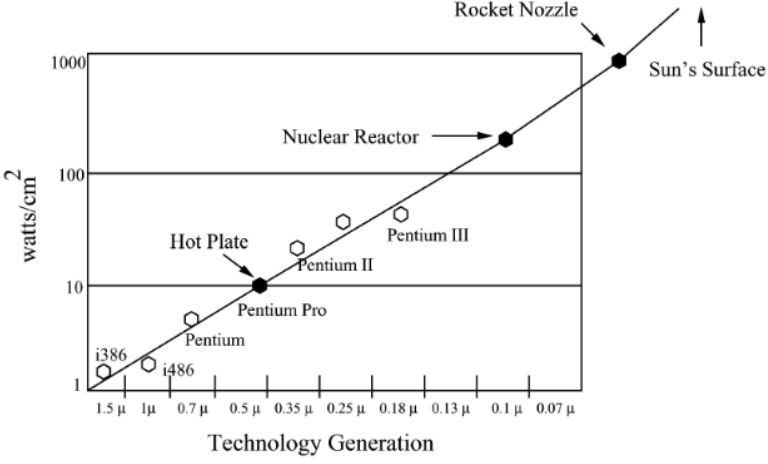
Heat sinks are often mounted over modern microprocessors. With miniaturization and the growth of frequencies, heat dispersion has become a significant problem. To understand this, refer to Figure 67 which shows the power density as a function of the technology.
The ASUS board of section 4.5, described on page 9, had the heat sink of Figure 68. It was mounted in contact with the microprocessor, with a thermal paste interposed for heat conduction. The heat sink is made up of a radial pattern of winglets, between which the air is moved by the fan. A heat- conducting paste is always placed between the processor and the face of the heat sink that comes into contact with it. This is to determine a uniform contact surface.
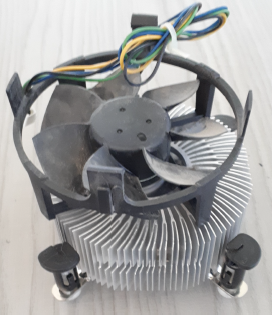
Figure 69 shows the overall heat sink system mounted on the microprocessor Core 2 Duo T5500 (inside the Vaio laptop VGN-1CZ). The heat sink consists of (i) a part that acts as a cover for the processor, (ii) a copper duct; and (iii) a sort of radiator over which the fan passes a flow of air. Schematically it works like this: the radiator is cooled by the airflow generated by the fan; consequently, heat is removed from the assembly formed by the duct and the processor cover.
Note that there is an additional heat duct that abuts the fan shell. This conductor comes from a heat sink located near the memory (not visible in the picture).
8.2. An optical mouse
The first mice were mechanical. A portion of a ball (with 2 degrees of freedom) emerged from the underside of the mouse; by moving the mouse the ball rotated and transmitted its movement to two wheels with orthogonal axes to which two encoders were associated, measuring the rotation speed (and therefore the movement along the axes of the two wheels). The mouse logic transmitted trains of pulses corresponding to the movements to the computer and therefore the mouse driver could reconstruct the position of the cursor. Mechanical mice had a significant flaw: they filled with dust, resulting in an impoverishment of their functioning.
Early optical mice used an LED and a photodiode to detect movement on the surface. To work, they required the supporting surface to be metallic with a dense network of thin blue lines.
Current optical mice still use an LED to generate light (the most refined ones use a laser to illuminate the support surface) and a very small camera for image acquisition. The camera is a CCD (Charge Coupled Device) sensor with a resolution of approximately 15×15 pixels on a surface of a few square millimeters. The output of the CCD is taken to a DSP (Digital Signal Processor) which carries out image processing. In practice, a comparison is made between the images detected at subsequent clocks, and the movement is calculated from the comparison, which is passed to the computer. All the logic in question, including the CCD and the interface to the computer is contained in a specific integrated circuit.
To function, unlike the first optical mice, the support surface must have irregularities, so that subsequent acquisitions differ from each other and the logic can determine if there has been movement. If the mouse is placed on a perfectly smooth surface, such as a sheet of glass, it will not work. Likewise, if you remove the mouse from the support surface and hold it up, it stops working.
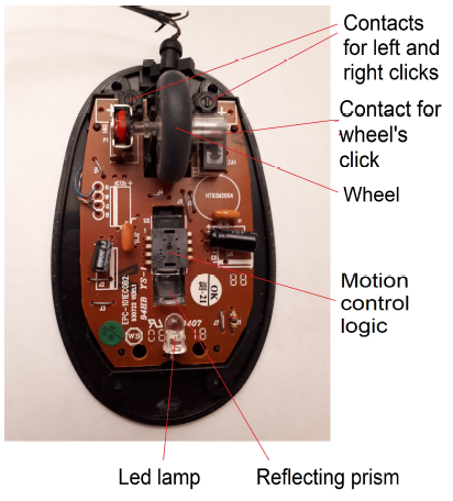
In Figure 70 the cover is removed. The figure highlights (a) the LED lamp, with a small prism in front that reflects the light towards the surface below; (b) the integrated circuit (Agilent ADNS-1610) containing the motion recognition logic; and (c) the mouse wheel with which the page is scrolled (it can also be clicked). The figure also indicates the contact points relative to the right or left click, as well as the contact point that recognizes the click on the wheel.
9. Conclusions
The described exhibit has been set up to evidenziate, the pace of advancement of the technologies related to computers. A large part of the described elements belonged, in the past, to the teachers in the Faculty; they were incorporated into the exhibit after they were abandoned due to obsolescence. The perspective is to continue to enlarge the collection, adding newer and, possibly, outstanding devices of the past.
Conflict of Interest The authors declare no conflict of interest.
- Wikipedia, “List of computer museums”, https://en.wikipedia. org/wiki/List_of_computer_museums, accessed on 2024-07-31.
- F. Faggin, M. E. Hoff, S. Mazor, M. Shima, “The history of the 4004”, IEEE Micro, vol. 16, no. 6, pp. 10–20, 1996.
- F. Faggin, “The making of first microprocessor”, IEEE Solid-state circuits, vol. 1, no. 1, pp. 8–21, 2009.
- G. Bucci, “Un percorso espositivo attraverso la tecnologia”, https: //sites.google.com/unifi.it/calcolatori-elettronici, ac- cessed on 2024-01-18.
- G. Bucci, “From a personal collection to an educational exhibit of the advancement of computer technology”, “Proceedings of Histelcon 2021”, pp. 54–57, 2021.
- Apple, “Apple unleashes M1”, https://www.apple.com/newsroom/ 2020/11/apple-unleashes-m1/, accessed on 2024-01-18.
- Apple, “Apple introduces M4 chip”, https://www.apple.com/ newsroom/2024/05/apple-introduces-m4-chip/, accessed on 2024- 07-31.
- MIT, “Development of magnetic core memory, 1950”, https://archivesspace.mit.edu/repositories/2/archival_ objects/142711, accessed on 2024-01-18.
- Wikipedia, “Olivetti elea”, https://en.wikipedia.org/wiki/ OlivettiElea, accessed on 2024-01-18.
- Morse, Raveiel, Mazor, Pohiman, “Intel Microprocessors–8008 to 8086”, Computer, vol. 13, no. 10, pp. 42–60, 1980.
- Intel, “Intel® 64 and ia-32 Architectures Software Developer’s Manual, Combined volumes”, https://www.intel.com/content/www/us/ en/developer/articles/technical/intel-sdm.html, accessed on 2024-07-31.
- AMD, “Amd Athlon™ 64 x2 Dual-Core Processor Product Data Sheet”, January 1980.
- IBM, “Powerpc 750 microprocessors”, https://www.ic72.com/pdf_ file/i/23704.pdf, accessed on 2024-07-31.
No related articles were found.