A Study on the Bromine-induced Corrosion/Defects in Wafer Fabrication
(This article belongs to the Section Electronic Engineering (EEE))
Export Citations
Cite
Younan, H. , Lois, L. J. , Lei, Z. , Binghai, L. and Xiaomin, L. (2024). A Study on the Bromine-induced Corrosion/Defects in Wafer Fabrication. Journal of Engineering Research and Sciences, 3(2), 8–14. https://doi.org/10.55708/js0302002
Hua Younan, Liao Jinzhi Lois, Zhu Lei, Liu Binghai and Li Xiaomin. "A Study on the Bromine-induced Corrosion/Defects in Wafer Fabrication." Journal of Engineering Research and Sciences 3, no. 2 (February 2024): 8–14. https://doi.org/10.55708/js0302002
H. Younan, L.J. Lois, Z. Lei, L. Binghai and L. Xiaomin, "A Study on the Bromine-induced Corrosion/Defects in Wafer Fabrication," Journal of Engineering Research and Sciences, vol. 3, no. 2, pp. 8–14, Feb. 2024, doi: 10.55708/js0302002.
For the semiconductor manufacturing processes, metal corrosion by halogen elements (e.g. fluorine, chlorine, and bromine) is always a critical issue. For the aluminum back-end-of-processes, these halogen elements tend to form aluminum halide defects on the surface of aluminum pads or aluminum metal wires, which can directly lead to the failure and reliability issues of the devices. While there have been some reports on the analysis and mechanisms of fluorine and chlorine pollution and their aluminum halide defects, there is a lack of research on the analysis and mechanism studies of bromine (Br) contamination and its associated aluminum bromide defects. In this work, we conducted the comprehensive study on Br-induced Al metal corrosion using Auger electron spectroscopy, scanning electron microscope and energy dispersive spectroscopy (SEM and EDS. Our study indicated that the Br-induced defects primarily consist of aluminum tribromide (AlBr3) and aluminum oxobromide (AlXBrYOZ), which are formed through a series of physical and chemical reactions. We propose a chain chemical reaction mechanism that is closely linked to the chemical corrosion processes induced by bromine.
1. Introduction
For the semiconductor manufacturing processes, there is always potential risk of contaminants generated from the production lines, such as tools, chambers and associated auxiliaries. These contaminants, particulate, or aerosol or molecular types, can seriously impact product and yield, degrade device performance and reliability, adversely affecting product manufacturability. Among these contaminants, halogen is commonly encountered, such as fluorine (F), chlorine (Cl), Br. These halogen elements can directly lead to the corrosion of the interconnect metal lines such as Al and Cu, forming aluminium halide defects. While there have been intensive studies on F and Cl induced metal corrosion [1-3], no much work was reported for the Br-indued metal corrosion and the associated mechanism.
This article aims to address this gap by conducting thorough analyses by using Auger Electron Spectroscopy (AES) and Scanning Electron Microscope (SEM) / Energy-Dispersive X-ray Spectroscopy (EDS), along with in-depth studies on the failure mechanisms induced by bromide on aluminium metal wires during wafer fabrication. Additionally, we propose a Br-chain chemical reaction mechanism that elucidates the Br-induced chemical corrosion processes.
In order to determine the underlying reasons behind the worm-like blemishes on aluminium metal wires, an analysis using Ion Chromatography (IC) was carried out. The purpose was to examine the extent of bromine contamination in the standardized mechanical interface (SMIF) pods. The findings revealed a significantly higher level of bromine content in the used SMIF wafer cassettes when compared to the new ones.
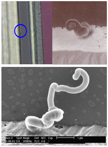
2. The Worm-Like Defects
The worm-like defects were caught by the inline YDD (yield defect density) after Al metallization processes. The inline defect map indicated that the defects were mainly in the wafer edge regions. Under the optical microscopy, the defect was shown as a small dot-like (the circled in Figure 1(a)), mainly existed along the edge of the Al metal lines. Further SEM analysis clearly showed that these small defects appeared as the worm-like, as shown in Fig.1 (b) and (c). These worm-like defects significantly impacted the quality and yield of the wafer fabrication process. Consequently, we proceeded to conduct a failure analysis and investigate the underlying mechanisms using various analytical techniques such as AES, SEM, EDS and ion chromatography (IC).
3. Failure Analysis Results and Discussions
To understand the chemical composition of the worm defects, further analysis was performed by using Auger Electron Spectroscopy (AES) and Scanning Electron Microscope (SEM) with Energy Dispersive X-ray Spectroscopy (EDS).
A.AES Analysis
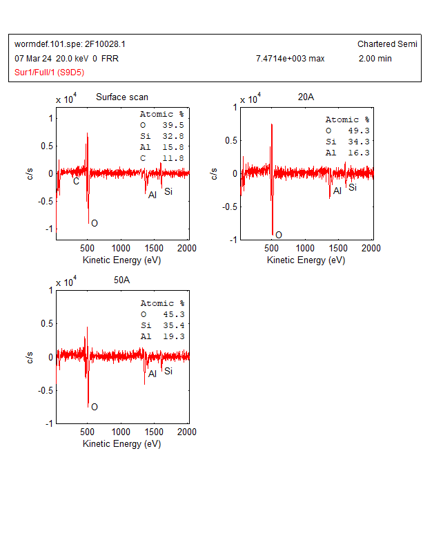
AES analysis was performed on the as-received sample surface (the top surface of sample), and sub-surface with surface layer removal of both 2nm and 5nm by Argon sputtering. These sputtering depths are estimated by using a Ta2O5 standard sample with the same sputtering conditions.
The relative atomic concentrations (at %) were derived from the Auger survey spectra. The values were calculated by first measuring elemental peak-to-peak heights in the survey scans and then applying sensitivity factors based on standard spectra of pure elements or selected compounds by using Eqn (1):
$$C_i = \frac{I_i}{(\text{Ist} \cdot \text{SD}_i)} \tag{1}$$
where Ii is the peak-to-peak amplitude of the element i from the test specimen, Istd is the peak-to-peak amplitude of the element i from the standard, Si is the relative sensitivity factor and Di is a relative scale factor between the spectra for the test specimen and standard.
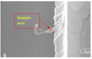
The AES wide scan was done on a worm-like defect and analysis area was shown in Figure 2. The AES wide scan results were depicted in Figure 3 (as received), Figure 4 (after 2nm sputtering) and Figure 5 (after 5nm sputtering), revealed the absence of any halogen element on the surface of the worm-like defect.

With the above Auger analysis, no halogen elements were detected. Therefore, further analysis is needed. In addition, there is still some uncertainty regarding the detection of bromine (Br) by Auger spectrum analysis due to the following reasons:

- The AES spectrum exhibits overlapping peaks for both bromine (1393 eV) and aluminium (1396 eV). This overlap creates a mere 3 eV difference, making it impossible for us to distinguish between these peaks accurately.
- The compound AlBr3, which includes bromine, is known to be water soluble. Therefore, we suspect that the AlBr3 present on the surface of the worm-like defects may have been washed away during the wafer fab process.
- Additionally, it is important to note that AES analysis solely provides information about the composition of the surface of the worm-like defects. It does not provide a comprehensive analysis of the entire sample. Consequently, based on the AES results obtained, we cannot definitively rule out the presence of bromine in the worm-like defects.
To further understand the chemical composition of the worm defects, EDS analysis was conducted.
B. EDS Analysis
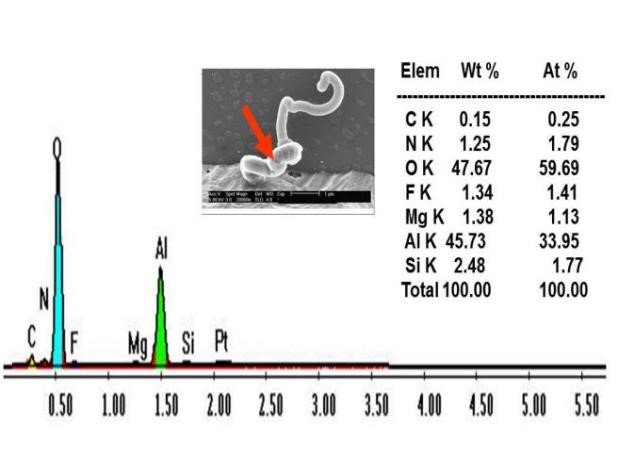
SEM/EDS analysis was performed at an acceleration voltage of 5kV, under which no chlorine (Cl) and bromine (Br) were detected. However, low content of fluorine (F) was detected, approximately 1.34 wt%, close to the detection limit of EDS, as shown in Figure 6.
Under 5 kV, the EDS is only capable of detecting the Lα peak of bromine at 1.4805 keV. However, this peak is overlapped with the Kα peak spectral line of aluminium at 1.4866 keV. Consequently, it is not possible to distinguish between these two peaks when using a 5 kV acceleration voltage. To identify the presence of bromine, we need to utilize the Kα peak spectral line of bromine at 11.9089 keV.
In our earlier research, we carried out an analysis on the selection of acceleration voltage in EDS (Energy-Dispersive X-ray Spectroscopy). Through our investigations, we discovered that an acceleration voltage of 5kV was insufficient to stimulate the Kα peak of bromine at 11.9089 keV. Consequently, we sought to determine the appropriate acceleration voltage required to excite the Br Kα peak at this energy level. To achieve this, we conducted a series of studies using both theoretical and experimental approaches [4-5].
At the first, according to the Duane-Hune law, we could derive a relationship between the electron beam acceleration voltage (Vi) and the energy of the characterization X-ray line (Ei):
$$V_i = k\,E_i \tag{2}$$
where Vi is the electron beam acceleration voltage, Ei is the energy of the characterization X-ray line and k is the constant of the over-voltage factor.
To determine the constant of the over-voltage factor (k), we conducted experiments using thin film layers of TiN and TiW, as well as Al bondpad samples. The characteristic lines of N Ka, Al Ka, Si Ka, W Ma, Ti Ka and W La peaks were used for studies during experiments.
During experiments, we varied the electron beam accelerating voltages from 1 to 20 kV. Additionally, we incrementally increased the beam accelerating voltage by 0.1 kV and then noted the corresponding voltages required when the characteristic lines of N Ka, Al Ka, Si Ka, W Ma, Ti Ka and W La peaks appeared.
We recorded the beam acceleration voltage required for each characteristic line to obtain a set of data, and then plotted the characteristic line energy as X axis and the acceleration voltage required for the characteristic lines as Y axis. Thus, the over-voltage constant, k, can be experimentally obtained.
The experimental results were shown in Figure 7 which revealed a strong linear relationship between the accelerating voltage (Vi) measured in kilovolts (kV), and the energy (Ei) of the characteristic X-ray line of the specific element of interest, measured in kiloelectron volts (keV). The over-voltage constant (k) was found to be approximately 1.42, as depicted in Figure 7.
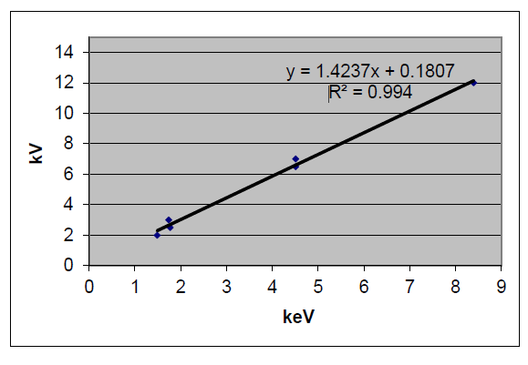
Figure 7 showed clearly a linear relationship between the beam accelerating voltage Vi (kV) and the energy of the characteristic X-ray line of the element interested Ei (keV). For the general application purposes, the k is recommended to be 1.5. Therefore, the acceleration voltage estimation formula is shown below:
$$V_i\ (\text{kV}) = 1.5\,E_i\ (\text{keV}) \tag{3}$$
where Vi is the beam accelerating voltage in kV used in the SEM/EDX, Ei is the energy of the characteristic X-ray line of the element interested in keV.
According to Eqn. (3), we understand that in order to excite the Kα line of bromine (11.9089keV), the acceleration voltage of EDS must be higher than 17.86 kV (1.5x the energy of the Kα line of bromine). Therefore, acceleration voltage of 20 kV is needed for the analysis of bromine in the worm-like defects. As a result, we detected the Kα peak of bromine on the worm-like defect as shown in Figure 8.
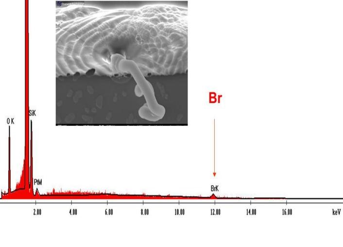
With the above analysis, the reason behind the non-detectability of Br (see Figure 6) was clear. It turned out that the Br peaks were not excited at the acceleration voltage of 5kV. To exciting the Br Ka line, we need to employ a higher voltage exceeding 17.86 kV, which is 1.5 times the energy of the Kα line of bromine. Therefore, it is advisable for us to utilize an acceleration voltage of 20 kV in order to accurately identify the Br Ka peak.
Henceforth, when conducting failure analysis through EDS in the future, we highly advise employing a combination of high acceleration voltage and low acceleration voltage simultaneously. By doing so, one can ensure the avoidance of any potential oversights in detecting elements.
4. Theoretical Model of Bromine-Induced Corrosion
The analysis conducted using high kV in EDS revealed the detection of bromine, thereby confirming its presence within the worm-like defects. The corrosion of aluminium wires and the subsequent formation of these worm-like defects were caused by contamination with bromine.
4.1. Br Contamination and Corrosion
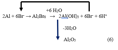
When contamination by Br takes place in a wafer fabrication facility, it leads to a chemical reaction between elements Br and Al, resulting in the formation of a compound known as Al bromide.:
$$\text{Al} + 3\text{Br}^- \rightarrow \text{AlBr}_3 + 3e^- \tag{4}$$
$$\text{or}$$
$$\text{Al} + 6\text{Br}^- \rightarrow \text{Al}_2\text{Br}_6 + 6e^- \tag{5}$$
(soluble in water)
4.2. Br-chain Chemical Reaction
In our previous investigation on Cl-induced corrosion, we put forward the notion of a chemical reaction involving a chain of chloride ions. Even a small quantity of chlorine was found to give rise to significant corrosion issues [3]. Similarly, we hypothesize that bromide ions could instigate a similar chain reaction. Aluminium bromide, being soluble in water, has the capability to release bromine ions when exposed to moisture. This, in turn, can lead to additional corrosion of aluminium wires. Consequently, even a minute amount of bromine contamination can repeatedly participate in chemical reactions, resulting in the creation of corrosion products.
$$n\text{Al}_2\text{O}_3 + m\text{Al}_2\text{Br}_6 \rightarrow \text{Al}_x\text{Br}_y\text{O}_z \ \text{(the worm-like defects)} \tag{7}$$
During the production process of wafer fabrication, an intriguing chemical reaction occurs involving the elements aluminium (Al) and bromine (Br), resulting in the formation of aluminium tribromide (AlBr3) or Al2Br6, which dissolves in water. Subsequently, when it comes into contact with water vapor, another chemical reaction takes place, leading to the generation of hydrogen bromide (HBr). This HBr compound then decomposes into bromine ions (Br ions) once again. The Br ions can then react with Al to produce more aluminium tribromide, thereby initiating a continuous cycle known as the “Br-chain chemical reaction.”
With this “Br-chain chemical reaction” progresses, a small number of Br ions repeatedly participate in chemical reactions, ultimately leading to highly intense corrosion reactions involving Br, even with a minimal number of Br ions present. Moreover, as a by-product of these chemical reactions, aluminium hydroxide is generated. During the production process, aluminium hydroxide undergoes dehydration and transforms into alumina. Through a series of physical and chemical reactions, these aluminium oxides, along with a portion of aluminium trichloride, combine to form a compound called aluminium oxobromide (AlxBryOz).
As the chemical reactions continue, the mixtures of alumina and aluminium oxobromide gradually increase, resembling the slow formation and emergence of the worm-like defects from the sides of Al metal wires. These noticeable defects become evident on the sides of Al metal wires. Ultimately, the interaction between alumina and aluminium bromide leads to the production of aluminium oxobromide (AlxBryOz). These compounds can grow alongside the sides of Al wires, particularly on wide Al metal lines (refer to Figure 6).
5. Root Cause Identification of Bromine Contamination
In order to address the issue of bromine contamination in the wafer fabrication processes, it is crucial to first identify its root cause. We understood that in the wafer fab front-end processes, HBr was used primarily for the polysilicon plasma etch. Typically, it was used alongside Cl2 and O2. Including HBr in the plasma etch chemistry is well known to lead to an improved etch profile, such as less undercut, more vertical sidewalls, and flatter trench bottoms. [6-9].
Upon thorough line investigation we have determined that the Br contamination was due to the cross-contamination from the standardized mechanical interface (SMIF) wafer cassettes through the production line. To pinpoint the source of bromine contamination, some of the SMIF wafer cassettes for Ion Chromatography analysis.
To measure the level of bromide in the SMIF pod, the inner surface of the pod was cleansed with high-purity deionized (DI) water. For surface contaminants, a straightforward method involving soaking the sample in DI water and manually agitating it can effectively extract these ionic contaminants. Subsequently, the Ion Chromatography technique was employed to quantify the bromine level present in the SMIF pod.
Ion Chromatography is a valuable method for analysing different ionic species in solutions. It relies on the principles of chromatographic separation and detection, with conductivity suppression being the most commonly used detection method.
5.1. Experimental
The technique of Ion Chromatography has found widespread application in the analysis of failures and monitoring of the environment in wafer fabrication. Previous research employed IC to ascertain the level of fluorine contamination in the foam material used for wafer packaging [1-2]. In this study, Ion Chromatography was utilized to determine the content of bromine (Br) in the SMIF pod. Two SMIF pods were examined, namely: (1) the affected pod and (2) the new pod. The new pod was used as a benchmark sample. Conversely, the affected SMIF pod had been utilized in the Fab process and is suspected to be contaminated by bromine.
5.2. Sample preparation
In order to ascertain the bromine content of the SMIF pod, the inner surface of the pod was cleansed using 400 ml of deionized water. To ensure optimal extraction of any ionic present on the surface, the pod was vigorously agitated for a continuous duration of 20 minutes. Subsequently, the water extract obtained from the pod was carefully transferred into a pristine sampling vial and subjected to analysis using an Ion Chromatograph.
5.3. Ion Chromatograph Analysis
The water sample obtained from the SMIF pods underwent analysis using the advanced DIONEX Reagent Free Ion Chromatography System (ICS-3000). This cutting-edge system is fitted with the state-of-the-art DIONEX IonPac AS-18 column and a highly efficient conductivity detector for optimal performance.
5.4. Ion Chromatograph Analysis and Results Discussions
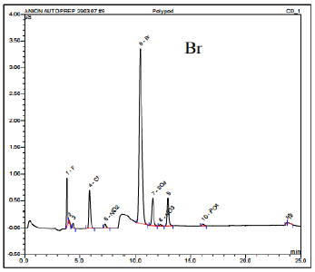
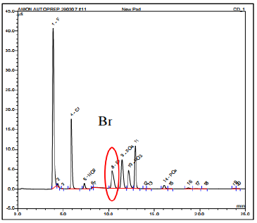
Based on the ion chromatography findings, the SMIF pod that was affected revealed the presence of F, Cl, and Br ions. Among them, the concentration of Br ion was the highest, measuring approximately 1.11 parts per million (ppm). Initially, the identification of bromide was challenging due to the detection of a broad peak at the same retention time as Br. This broad peak could be an unknown substance overlapping with the Br peak, or it could be Br ion present in high concentration.
To validate the existence of Br, a diluted sample was prepared by mixing it with deionized (DI) water at a ratio of 100:1. After dilution, the broad peak was confirmed to be the Br peak. The IC spectrum in Figure 9 exhibits the diluted IC analysis of the affected SMIF pod.
Similarly, a new pod underwent the same analysis, and a low level of Br was detected, measuring approximately 16 parts per billion (ppb). This concentration is significantly lower, around 70 times, compared to the affected SMIF pod. The IC spectrum in Figure 10 demonstrates the IC analysis of the new pod.
The IC findings from both pods strongly suggest that the contamination of the affected SMIF pod occurred during the wafer fab process. This contamination could potentially be attributed to cross-contamination from the environment or the chemical solvents employed in the wafer fab process. The results have been communicated to the responsible individuals in charge of the fab facility for their thorough examination and evaluation.
The level of bromine pollution found in the previously utilized SMIF wafer cassettes (depicted in Figure 9) was roughly 70 times greater when compared to the fresh SMIF wafer cassettes (depicted in Figure 10). The results obtained from the analysis of ion chromatography indicate that the affected SMIF pod was contaminated by Br during the wafer fab process. It is possible that there was cross contamination either from the surrounding environment or from the chemical solvents used in the wafer fab process, particularly during the Front-end-of-line (FEOL) processing stage. If the contaminated pod was used during the Back-end-of-line (BEOL) processing, it is likely that the presence of Br caused contamination in the metal lines, leading to Br-induced corrosion and the formation of the worm-like defects.
6. Conclusion
In this work, we have conducted a thorough study on the Br-induced Al metal corrosion and the associated mechanism of the worm-like defect formation by using various analysis techniques, such as AES, SEM/EDS, and Ion chromatography.
By closely collaborating with the wafer fab processing team, we have successfully identified the root cause of the contamination issue and effectively eradicated the presence of bromine. Furthermore, we have delved into the underlying mechanisms of failure induced by Br-induced corrosion. Our research has proposed a chemical reaction mechanism involving a chain of bromine atoms, closely associated with the chemical corrosion processes triggered by bromine. According to our proposed mechanism, the defects induced by bromine primarily consist of aluminium tribromide (AlBr3) and aluminium oxobromide (AlxBryOz). These compounds are formed through a series of physical and chemical reactions. By conducting extensive surface analysis and investigating the mechanisms of bromine contamination and its impact on aluminium metal wires, our objective is to contribute to a deeper comprehension of these critical issues in the field of semiconductor wafer manufacturing. The examination of bromine-induced defects in wafer fabrication has provided insights into the underlying mechanisms and offered valuable information for effective strategies to eliminate them. By implementing targeted measures such as process modifications, protective measures, and optimized parameters, manufacturers can mitigate the adverse effects of bromine-induced defects, leading to enhanced wafer quality and increased overall yield.
It has been confirmed that the corrosion of the metal occurred as a result of bromine contamination, resulting in the formation of the worm-like defects known as AlxBryOz on the sidewalls of the aluminium metal lines. It is highly suspected that the contamination with bromine occurred through cross-contamination between the front and backend processes via the SMIF pods. In response, the process engineer has implemented measures to control the use of SMIF pods between the front and backend processes and has introduced a cleaning procedure.
In this article, we thoroughly explore the process of determining the optimal acceleration voltage for EDS analysis. Specifically, we focus on selecting an acceleration voltage that is 1.5 times higher than the energy level of the Kα line of bromine.
Conflict of Interest
The authors declare no conflict of interest.
Acknowledgment
The authors would like to thanks FA personnel from Wintech-Nano for their technical support.
- Y. N. Hua, S. Redkar, C. K. Lau, Z. Q. Mo; November 3–7, 2002. “A Study on Non-Stick Aluminium Bondpads Due to Fluorine Contamination Using SEM, EDX, TEM, IC, AUGER, XPS and TOF-SIMS Techniques.” Proceedings of the ISTFA 2002. ISTFA 2002: Conference Proceedings from the 28th International Symposium for Testing and Failure Analysis. Phoenix, Arizona, USA, pp. 495-504, 2002, DOI:10.31399/asm.cp.istfa2002p0495
- Y. N. Hua, S. Redkar, Ron Dickinson, S. L. Peh, Shirley; November 2–6, 2003. “A Study on Fluorine-Induced Corrosion on Microchip Aluminum Bondpads.” Proceedings of the ISTFA 2003. ISTFA 2003: Conference Proceedings from the 29th International Symposium for Testing and Failure Analysis. Santa Clara, California, USA, pp. 249-255, 2003, DOI:10.31399/asm.cp.istfa2003p0249
- Y. Hua, L. Liao, L. Binghai, L. Zhu and X. Li, “Failure Analysis & Mechanism Studies of the Worm-like Defects in Vias of Wafer Fabrication,” 2021 IEEE 23rd Electronics Packaging Technology Conference (EPTC), Singapore, Singapore, pp. 50-52, 2021, doi: 10.1109/EPTC53413.2021.9663918.
- Hua Younan, Liu Binghai, Mo Zhiqiang and J. Teong, “Studies and applications of standardless EDX quantification method in failure analysis of wafer fabrication,” 2008 15th International Symposium on the Physical and Failure Analysis of Integrated Circuits, Singapore, pp. 1-6, 2008, doi: 10.1109/IPFA.2008.4588206.
- Y. Hua et al., “Studies of Determination Method of TiN Residue on Al Bondpads,” 2023 IEEE International Symposium on the Physical and Failure Analysis of Integrated Circuits (IPFA), Pulau Pinang, Malaysia, pp. 1-4, 2023, doi: 10.1109/IPFA58228.2023.10249105.
- M. A. Vyvoda, H. Lee, M. V. Malyshev, F. P. Klemens, M. Cerullo, V. M. Donnelly, D. B. Graves, A. Kornblit, J. T. C. Lee; Effects of plasma conditions on the shapes of features etched in Cl2 and HBr plasmas. I. Bulk crystalline silicon etching. Journal of Vacuum Science & Technology A, vol. 16, no. 6, pp. 3247–3258, 1998, DOI:10.1116/1.581530
- W-H. Lo and W-C. Wang, “HBr Silicon Etching Process,” U.S. Patent 6,358,859 B1, (March 19. 2002). 8.
- Hydrogen Bromide 4.5 [Specification sheet], Praxair, document EG 48–4.5 08/2003. 9.
- Hydrogen Bromide [Specification sheet], Air Liquide America Specialty Gases