MC-SPWM and MC-THIPWM Methods for Symmetric and Asymmetric Design of CHB-MLI: A Study
(This article belongs to the Special Issue on SP1 (Special Issue on Multidisciplinary Sciences and Advanced Technology 2022) and the Section Electrical Engineering (ELE))
Export Citations
Cite
Patel, J. and Sood, V. (2022). MC-SPWM and MC-THIPWM Methods for Symmetric and Asymmetric Design of CHB-MLI: A Study. Journal of Engineering Research and Sciences, 1(4), 148–160. https://doi.org/10.55708/js0104017
Jigneshkumar Patel and Vijay Sood. "MC-SPWM and MC-THIPWM Methods for Symmetric and Asymmetric Design of CHB-MLI: A Study." Journal of Engineering Research and Sciences 1, no. 4 (April 2022): 148–160. https://doi.org/10.55708/js0104017
J. Patel and V. Sood, "MC-SPWM and MC-THIPWM Methods for Symmetric and Asymmetric Design of CHB-MLI: A Study," Journal of Engineering Research and Sciences, vol. 1, no. 4, pp. 148–160, Apr. 2022, doi: 10.55708/js0104017.
Cascaded H-bridge multilevel inverters (CHB-MLI) are employed in a variety of medium/high power applications. These inverters are known to inject unwanted harmonics into the grid, which negatively affects the grid and connected loads. CHB-MLI topology can reduce many of these harmonics by producing multiple output voltage levels and improves the fundamental component using a suitable modulation technique. However, the CHB-MLI topology configuration requires multiple isolated input sources which must be balanced either with the modulation technique or with an additional method. This paper analyzes multi-carrier pulse width modulation (MC-PWM) techniques for CHB-MLIs. In this study, two basic configurations of CHB-MLI symmetrical and asymmetrical are reviewed, followed by their mathematical analysis. Also, this paper analyses multi-carrier based sinusoidal pulse width modulation (MC-SPWM) and multi-carrier based third-harmonic injected pulse width modulation (MC-THIPWM) techniques with phase-shifted (PS) and level-shifted (LS) carrier arrangements for the CHB-MLI. Moreover, a simulation study has been conducted using MATLAB Simulink to analyze the performance of MC-PWM techniques for the symmetrical and asymmetrical type CHB-MLIs. The 7-level and 9-level CHB-MLIs were evaluated for the stated MC-PWM techniques in terms of harmonics and fundamental components. In addition, discharging current of all input sources was checked to verify the ability of all MC-PWM techniques to balance all input sources.
1. Introduction
High-voltage (HV) converters are used in motor drives [1], static VAR compensators [2], renewable energy systems [3], [4], high-voltage direct current (HVDC) transmission and other similar applications [5–7]. The traditional single-phase inverter generates two or three-levels in the output signal, while MLIs can create multi-levels in the output signal. More levels supply a lower distortion and better-quality output signal. Moreover, the MLI topology provides a precise control of the voltage stresses on each switch [8]. Therefore, the MLI is more suitable for medium/high voltage and high-power applications. Although there are many MLI topologies available [9–11], the most prevalent MLI topologies are neutral point clamped MLI (NPC-MLI) [4], [12], [13], flying capacitor MLI (FCMLI) [14], and cascaded H-bridge MLI (CHB-MLI) [15]. Among these MLIs, the CHB-MLI has acquired special attention in most topologies because of the modular structure and flexible to generate any number of output voltage levels [16–18].
The CHB-MLI is easy to construct and highly dependable. This inverter has either a symmetrical or asymmetrical mode of operation [19], [20]. The symmetrical mode of CHB-MLI utilizes equal-amplitude DC sources. In contrast, the asymmetrical form of CHB-MLI uses the unique amplitude of various DC voltage sources. Also, the asymmetrical form of CHB-MLI utilizes fewer power electronic (PE) switches than the symmetrical type CHB-MLI [21]. All PE converters need a suitable PWM technique for their operation.
The main classifications of PWM techniques are low- and high-frequency (HF) switching modulation techniques to control multi-level inverters [22], [23]. The low-frequency (LF) modulation technique is more suitable for the high-power converter in high voltage applications like HVDC transmission. The nearest-level modulation (NLM) and selective harmonics elimination (SHE) methods are placed in this category [24], [25]. These methods are efficient in reducing the switching losses. The NLM method is also known as the staircase modulation technique since it generates the nearest possible level by comparing a sinusoidal reference with carriers [26]. This method is suitable for implementing with a larger number of modules. The converter’s performance diminishes, and total harmonic distortion (THD) improves when fewer modules are obtainable with this method [27]. This method was also combined with the space-vector modulation technique to improve its capability [28], [29].
Another LF method is the SHE method. In this method, the solution of a set of non-linear transcendental equations are the switching angles of the pulses which turn ON/OFF the PE switches [30], [31]. The primary goal of this method is to cut specific lower-order harmonics from the output voltage/current waveforms. Also, this method can control PE switches at the fundamental frequency, which lowers the switching losses [32], [33]. The trigonometric terms are used in this method to express harmonic components.
The number of equations increases because the switching angles increase with the higher number of modules. The authors of [30], [34–36] proposed many equation-solving methods like the Newton-Raphson (NR) method, particle swarm optimization (PSO), and genetic algorithms (GA) to ease the calculation of the switching angles. Regardless, it is challenging to solve these non-linear equations for more modules. Moreover, output signal and dynamic response are weak [30], [37].
The space vector PWM (SV-PWM) is also a LF switching technique. This method is an addition to the basic SV control technique with an expanded number of vectors [38]. This method provides a higher voltage on the AC side [39]. At the same time, it reduces the voltage and current THD compared to the SPWM method. The functional status of the switches can be described by switching states for this method. Yet, it is very complicated to decide the whole the vectors for more modules in HV applications [40], [41].
The carrier-based modulation technique is considered a HF modulation scheme. A single HF triangular carrier wave is compared with the reference wave to generate gate pulses [42]. It is also known as the SPWM technique. It is simple and easy to implement and highly popular.
Some researchers [43–46] replaced the triangular carrier signal with the other carrier signals to develop new modulation techniques. In one technique, the sinusoidal wave replaces the traditional carrier signal. This method is known as sinusoidal-SPWM (S-SPWM). This technique produced more harmonics with a lower fundamental output voltage than the SPWM technique [43]. The inverse sinusoidal carrier PWM (ISCPWM) method is the other technique, which generates switching pulses using an inverse sinusoidal carrier signal. This method increases the fundamental component in the output signal [43], [44], [46], [47]. Later it was changed to the variable frequency inverse sinusoidal PWM (VFSPWM). Both methods require high computational power digital hardware since it needs a smaller time step to generate a complex carrier signal [44]. These carrier signals and modulation signals must be synchronized to control harmonics. Another advanced carrier-based PWM technique, named UN-shape carrier PWM (UNPWM) [43], was proposed to overcome the drawbacks of SPWM and S-SPWM. It can increase the essential component and reduce harmonics in the output signal, though generating an UN-shape carrier signal is not easy with digital controllers.
As in the conventional method, gating pulses result from corresponding multiple carrier signals and sinusoidal reference signals. The MC-PWM technique for the MLI is an extension of this traditional technique. The third harmonic injected PWM (THIPWM) method uses a newly generated reference signal. This reference signal is achieved by injecting the third-order harmonic into the sinusoidal signal [48], [49].
Like the SPWM, switching pulses are produced with the triangle and a new reference signal. In both (SPWM and THIPWM) methods, HF carrier signal transfers the LF harmonics to HF harmonics. The affordable filter can decrease these HF harmonics to the accepted harmonic limits suggested by the IEEE Std 519-1992. According to IEEE Std 519-1992, the total voltage distortion (THD) limit is 5% for the voltage 69 kV and below [50], [51]. Furthermore, the fundamental element becomes lessened in the output by the MC-SPWM technique regarding MC-THIPWM. Therefore, MC-SPWM reduces the inverter’s efficiency [52].
There are two ways to arrange carrier signals in the MC-PWM method: phase-shifted (PSPWM) or level-shifted (LSPWM). In the PSPWM, the phase of the one carrier signal displaces the other signal’s phase horizontally. In contrast, one carrier signal shifts the other vertically in the LSPWM. Moreover, the carrier signals are placed as alternate-phase-disposition (APOD), in-phase-disposition(IPD), and phase-opposition-disposition(POD) [53–57].
This paper investigates the behavior of a 7-level and 9-level 3-phase symmetric/asymmetric CHB-MLI using MC-based SPWM and THIPWM methods for all carrier signal arrangements. This paper is arranged as follows: Section 2 introduces an H-bridge inverter. Section 3 presents the CHB-MLI topology. The MC-based PWM approach is illustrated in Section 4. Similarly, the execution for the symmetric and asymmetric types of CHB-MLI is presented in Section 5. Then, a qualitative analysis and numerical examination of both kinds of CHB-MLI using different MC-PWM is produced, employing MATLAB/Simulink simulations.
2. H-bridge inverter
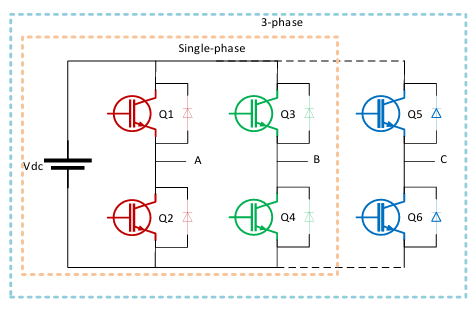
The traditional low voltage (LV) inverter (voltage source inverter (VSI)) is a 1-phase, which produces two-level in the output, which is used for LV applications. A classic configuration of a 1-phase H-bridge (HB) inverter is shown inside the orange square in Figure 1. This VSI is simple and effortless to run. A suitable control method can be used with this VSI to generate the 3-level signal in the output. There are 4-switches used to form 2-legs of the HB. The 3-phase inverter (shown in Figure 1 inside the blue box) has 6-switches to build 3-legs for phases A, B & C respectively.
$$v_o = \frac{4V_{dc}}{\pi} \left( \sin(\omega t) + \frac{1}{3} \sin(3\omega t) + \frac{1}{5} \sin(5\omega t) + \cdots \right) \tag{1}$$
Where: Vdc is a DC voltage
The peak of the fundamental element is shown in Eq. (2), and the value of the root mean square (RMS) signal is expressed in Eq. (3).
$$V_{o1\_peak} = \frac{4V_d}{\pi} \approx 1.27V_{dc} \tag{2}$$
$$V_{o1\_rms} = \frac{v_{o1p}}{\sqrt{2}} = \frac{2\sqrt{2}V_d}{\pi} \approx 0.9V_{dc} \tag{3}$$
Where: V01_peak is the highest value of the produced voltage is V01_rms RMS voltage
3. Configuration of cascaded h-bridge inverter
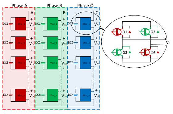
The applications of HV cannot use 1-phase LV inverters since the restricted voltage blocking capacity of semiconductor switches. Therefore, the CHB-MLI topology is fitting for these types of applications. Figure 2 illustrates the 3-phase CHB-MLI. This configuration uses several HB modules/cells connected in series to produce an enhanced AC output voltage with lower harmonic contents.
Based on the DC source configuration, there are two ways to implement the CHB-MLI symmetrical or asymmetrical configurations.
3.1. Symmetrical configuration
The symmetrical design of CHB-MLI uses multiple isolated DC sources with identical amplitudes. Similarly, a CHB-MLI with 3-series connected cells uses isolated DC input sources of the same amplitudes to produce a 7-level output signal. These 7-levels are measured as 0, ±E, ±2E, and ±3E. Usually, the following equation is used to decide the number of levels in this configuration:
$$M = (2H + 1) \tag{4}$$
Where “M” describes the maximum levels in the output signal and “H” relates the number of HB cells per leg.
3.2. Asymmetrical configuration
The asymmetrical type CHB-MLI uses various scale isolated DC sources. Each cell produces 3-different voltage levels in this sort of structure. Therefore, the highest voltage levels depend on the DC sources’ peak value. There are binary and trinary systems to figure out DC levels in a CHB-MLI. In the binary method, it uses Vdc1 = E, Vdc2 = 2E, and Vdc3 = 4E. This sequence of input amplitudes of voltages results in 15 levels in the phase-voltage of CHB-MLI. Eq. (5) denotes the output voltage-level in this design.
$$M = (2^{H+1} – 1) \tag{5}$$
In trinary method, all input sources are set as: Vdc1 = E, Vdc2 = 3E, and Vdc3 = 9E. This configuration produces voltages with 27-levels in the output phase signal. Eq. (6) expresses the upper limit of output signal levels.
$$M = 3^H \tag{6}$$
4. Mathematical analysis
In a CHB-MLI, the voltage difference of PE switches is each cell’s output voltage. Then, two individual switching functions control each cell and Eq. (7) sets the voltage level in each cell \(V_{o\_cell_i}\) as:
$$V_{o\_cell_i} = V_{dc}(Q_{1\_cell_i} – Q_{3\_cell_i}) \tag{7}$$
Where switching functions are \(Q_{1\_cell_i} \text{ and } Q_{3\_cell_{i’}}\) and Vdc is a DC input of each HB.
A switching function, Qi is defined as Eq. (8) where i =1, 2, ···, n..
$$Q_i = \begin{cases}
1; \text{ when } Q_i \text{ is ON} \\
0; \text{ when } Q_i \text{ is OFF}
\end{cases} \tag{8}$$
The overall output voltage of a CHB-MLI is produced as shown in Eq. (9) for the symmetric structure, and Eq. (10) for the asymmetric configuration.
$$V_o = V_{dc} \sum_{i=1}^{n}(Q_{1\_cell_i} – Q_{3\_cell_i}) \tag{9}$$
$$V_o = \sum_{i=1}^{n} (Q_{1\_cell_i} – Q_{3\_cell_i}) V_{dc_i} \tag{10}$$
Thus, Eq. (11) shows the 7-level symmetric CHB-MLI’s output voltage.
$$\left\{
\begin{aligned}
V_{o1} &= V_{dc}(Q_{1\_cell_1} – Q_{3\_cell_1}) \\
V_{o2} &= V_{dc}(Q_{1\_cell_2} – Q_{3\_cell_2}) \\
V_{o3} &= V_{dc}(Q_{1\_cell_3} – Q_{3\_cell_3})
\end{aligned}
\right. \tag{11}$$
Similarly, Eq. (12) illustrates the output voltage of 15- and 27-level asymmetric CHB-MLIs.
$$\left\{
\begin{aligned}
V_{o1} &= V_{dc_1}(Q_{1\_cell_1} – Q_{3\_cell_1}) \\
V_{o2} &= V_{dc_2}(Q_{1\_cell_2} – Q_{3\_cell_2}) \\
V_{o3} &= V_{dc_3}(Q_{1\_cell_3} – Q_{3\_cell_3})
\end{aligned}
\right. \tag{12}$$
5. MC-PWM methods for symmetric and asymmetric CHB-MLI
The MC-PWM methods are named PSPWM and LSPWM as per classification.
5.1. PS-PWM
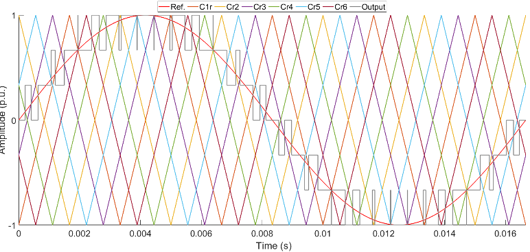
A CHB-MLI with “(M-1)” carrier-signals can produce an “M” number of levels in the output voltage. These carrier signals have equal amplitude and frequency. Nevertheless, there is a phase displacement between the two carrier waves. The Eq. (13). helps to decide the phase displacement angle for the carrier signals. The PS-PWM method can be sinusoidal PSPWM (PSSPWM) or third harmonic injected PSPWM (THIPSPWM) based on the reference signal.
$$\phi_{cr} = \frac{360}{(M – 1)} \tag{13}$$
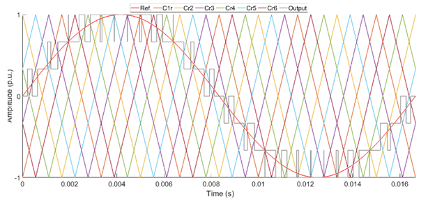
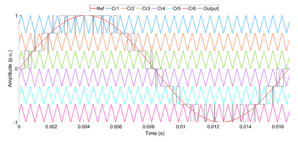
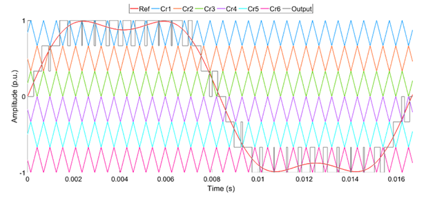
Figure 3 shows the PS-SPWM method for a 7-level CHB-MLI. In this figure, six carriers (Cr1 – Cr6) are shown. Also, the sinusoidal reference wave is used with carrier waves to create control pulses for the PE switches. Furthermore, the gray color waveform approximates the 7-level CHB-MLI’s output voltage.
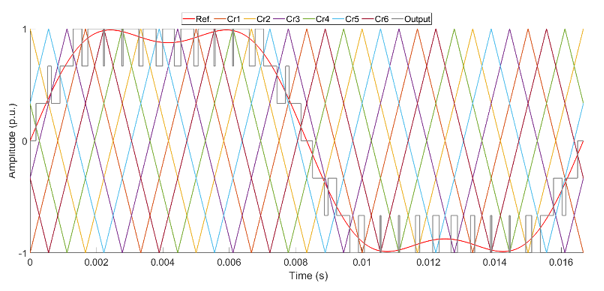
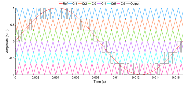
Like the PSSPWM, THIPSSPWM has (M-1) carrier signals for the M-level of CHB-MLI (Figure 4). However, in this method THI signal is used as a modulation signal to generate switching pulses for the inverter. Also, the signal in gray color estimates the output phase voltage. A 3-phase system is proper for this control method because the triplen harmonics do not appear when a delta-connected transformer is placed.
Also, each HB can produce output voltage (where i = 1, 2, 3…. N). The Eq. (14) describes 7-level CHB-MLI’s output voltage (VAN ).
$$v_{AN} = v_{H1} + v_{H2} + v_{H3} \tag{14}$$
Eq. (15) describes the simplified form of CHB-MLI’s switching frequency for PSPWM system.
$$f_{inv} = 2H f_{sw} = (M – 1)f_{sw} \tag{15}$$
A symmetrical configuration is suitable for operating using the PS-PWM method because it benefits balancing all DC sources.
5.2. LS-PWM
Like the PSPWM, LSPWM needs “(M-1)” carrier waves that are equal in amplitude to produce “M” levels in the output voltage. Regardless, there is vertical displacement in each other’s position such that the bands they inhabit are bordering. Furthermore, LSPWM is classified as LSPWM and THILSPWM. Also, carrier waves can be arranged in various forms, namely, in-phase disposition SPWM (LSIPDSPWM), level shifted alternate phase-disposition SPWM (LSAPODSPWM), and level shifted phase-opposition-disposition (LSPODSPWM). All the above LSPWM techniques are shown in Figures 5 to 10.
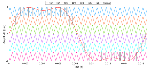
The phase displacement between two carrier waves is zero in the LSIPDSPWM. In contrast, there is 180° phase displacement between every carrier wave in LSAPODSPWM. In the LSPODSPWM, the carrier waves are in phase, placed above zero-reference. Similarly, the carrier waves are in phase, placed beneath zero-reference. However, the 180° phase displacement is seen between the above-zero and below-zero reference lines. A sinusoidal reference wave is used in all three methods. Also, the gray color signal estimates the output voltage.
The control pulses for HB1 can be generated by the uppermost and lowest carrier waves. Similarly, the pulses can be generated for HB3 and HB2 with the innermost carrier waves. The estimation of the output wave and the arrangements for the 7-level CHB-MLI is shown in Figures 5 to 10.
Eq. (16) describes the output voltage of a 7-level CHB-MLI. Also, it shows the peak output voltage for each HB.
$$v_{AN} = v_{H1} + v_{H2} + v_{H3} \tag{16}$$
The operating frequency of PE switches in HB1 is the product of reference wave frequency and the switching pulses per cycle. Furthermore, the switching frequency is different in another HB module. The HB3 can be run at the most subordinate switching frequency.
In general, the operating converter frequency using the LSPWM is equal to the carrier frequency (fcr ).
$$f_{sw,conv} = f_{cr} \tag{17}$$
Eq. (18) shows the average value of operating frequency for switches
$$f_{sw,dev} = \frac{f_{cr}}{(m – 1)} \tag{18}$$
The PSPWM method generates each HB module’s equal amplitude output signal with small phase displacement. Also, the current-carrying time is identical for all switches. In contrast, the output waveforms are not identical when HB modules are controlled by the LS-PWM method because of the different current-carrying times. This issue can be solved with a proper balancing technique to balance losses and conduction time. However, this increased process expands the complexity and price of the design.
6. Realization of MC-PWM for CHB-MLI
MC-PWM technique controls symmetric/asymmetric type CHB-MLI. The “(M-1)” carrier waves can produce “M” level output voltage for both types of CHB-MLI.
The PSPWM technique is applied to the symmetric CHB-MLI only since it balances load current among all isolated inputs. In contrast, the LSPWM method cannot balance the load current among all sources in both types of CHB-MLIs. Still, the load balancing technique is not used in this study.
In the PSPWM method, a 60º phase shift between two carrier waves is needed to produce a 7-levels output voltage for the symmetrical type CHB-MLI configuration.
Likewise, a 45º phase shift is needed to generate a 9-level output voltage. A sinusoidal modulation wave is used to form ad PSPWM technique, and a THI modulation wave is considered to create the THIPSPWM method. The THI wave is generated by injecting a third harmonic wave into the 60 Hz frequency sinusoidal wave. The modulation wave is compared with the carrier waves to produce control pulses for the PE switches in both methods.
Both symmetric and asymmetric structure of CHB-MLI model is created considering the LSPWM method. In this method, “(M-1)” carrier waves are vertically displaced to produce an “M” level output signal.
In the LSPWM method, each carrier signal’s peak-to-peak value (PPV) can be decided by using Eq. (19).
$$\text{PPV} = \texttt{“1/(NC/2)”} \tag{19}$$
Where NC is a sum of all carrier waves.
The PPV per carrier wave was 0.33 in symmetrical type 7-level CHB-MLI. Hence, three carrier wave was placed above 0 references, and the remaining three were placed under 0 reference. So, the range of carrier waves is 0.67 to 1 for Cr1, 0.33 to 0.67 for Cr2, and 0 to 0.33 for Cr3. Similarly, the three carriers below 0 reference hold the same values but with negative polarity. Eq. (19) shows that the 9level symmetric type CHB-MLI used a 0.25 PPV value.
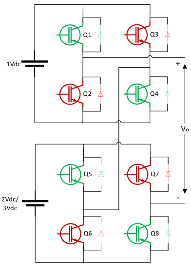
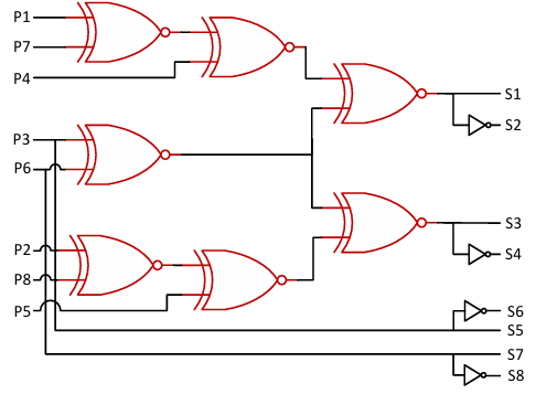
Figure 11 shows the asymmetrical configuration of CHB-MLI. This design has fewer switches than symmetrical CHB-MLI despite an equal number of carrier waves being needed. Consequently, an added circuit is needed for further processing these waves to produce switching pulses. The 7-levels in the output signals are, +3E, +2E, +E, 0, -E, -2E, and -3E. These values are output achieved by processing six carrier waves using source formation of 1:2 ( = E, = 2E). Figure 12 describes the logic circuit which generates the control pulse for this design. Likewise, the eight carrier waves are used to achieve 9-levels, +4E, +3E, +2E, +E, 0, -E, -2E, -3E and -4E, with 1:3 source composition ( Vdc1 = E, Vdc2 = 3E). Figure 13 shows the control pulse logic circuit for this design.
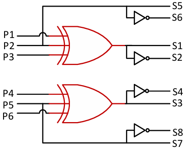
The comparison of carrier and modulation waves produced the switching pulses (P1-P6). As discussed earlier, six carrier waves are used to produce a 7-levels output signal. The modulating wave either be a sinusoidal wave or a THI wave. Figure 12 describes the further processing of these pulses. The pulses P1, P2, and P3 are used as input to the XOR, producing control signal S1 and complimentary signal S2. Thus, S1 and S2 connect to the switches Q1 and Q2. Signal P2 is used for S5 and complementary signal to S6. Another XOR gate used P4, P5, and P6 as input signals. This logic gate produces S4 and complimentary signal S4, which are connected to the switches Q3 and Q4. The signal S7 for switch Q7 is connected to P5, and S8 has used the complementary pulse of P5 for switch Q8.
Asymmetric type CHB-MLI in 9-level design, eight pulse waves P1 to P8 are produced with a single modulating and eight carrier waves. These pulses are further processed using logic gates shown in Figure 13. Signals S1 and complimentary signal S2 are produced with the P1, P3, P4, P6, and P7 input pulses for the NXOR logic. The S1 and S2 drive the switches Q1 and Q2. Likewise, another NXOR logic is used to produce driving pulses S3 and complimentary pulse S4. In this process, P2, P3, P5, P6, and P8 are employed as input signals for the NXOR logic. Also, the driving pulses S5 and S7 are connected to P3 and P6. Moreover, the control pulse S7 is complimentary to S8, and S6 is complimentary to S5.
7. Simulation results
MATLAB/Simulink models are used to study MC- SPWM and MC-THIPWM methods for a symmetrical and asymmetrical design of 3-phase CHB-MLI.
The symmetrical 7- and 9-levels 3-phase CHB-MLI are integrated with MCPWM methods, PSSPWM, PSTHIPWM, LSSPWM, and LSTHIPWM. All MCPWM methods are evaluated by examining the THD and fundamental signals in the line-to-line (L-L) output voltage. The operating frequency of the inverter (fsw_inv) is 96 times the essential frequency of 60 Hz (i.e., 5760 Hz).
Then, asymmetrical 7- and 9-levels 3-phase CHB-MLI operated using variation of LSSPWMs (LSIPDSPWM, LSAPODPWM & LSPODSPWM) and THILSPWM (THILSIPDPWM, THILSAPODPWM & THILSPODPWM) methods. The THD and fundamental components are analyzed using all six various of LSPWM. Furthermore, a qualitative, and quantitative assessment is carried out for all MCPWM methods for both design of CHB-MLI.
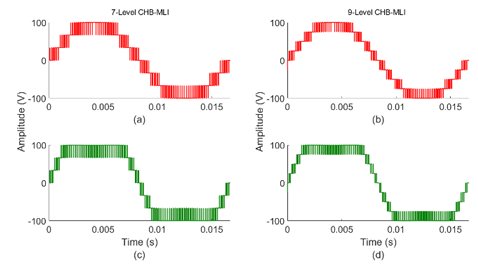
The output phase voltage of 7- and 9-levels CHB-MLI is shown in Figure 14 ((a)-(d)) for PSSPWM and THIPSPWM methods. PSPWMs methods generate an output signal that is like the sinusoidal signal in the form of staircase. Additionally, CHB-MLI produces output voltage of 100 V with both control methods. Also, the examination of output signal generated by THIPSPWM shows, the peak voltage created stays constant for an extended time as compared to the signal generated by the PSSPWM method.
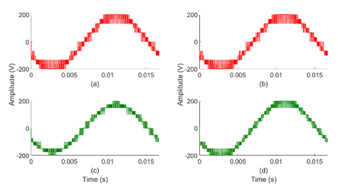
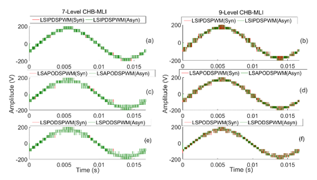
The L-L voltage of the 7- & 9-levels CHB-MLI is shown in Figure 15 ((a)-(d)). These inverters are run with PSSPWM and THIPSPWM methods like the phase voltage. Both methods produce equal peak voltages.
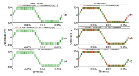
The overlaid waveforms of phase voltage (Figure 16 (a)-(f)) produced by symmetrical and their corresponding asymmetrical design of 7- & 9-level CHB-MLIs controlled with each LSPWM method under study. Like the PSPWM method, CHB-MLI create 100 V peak in the output signal with all LSPWM methods.
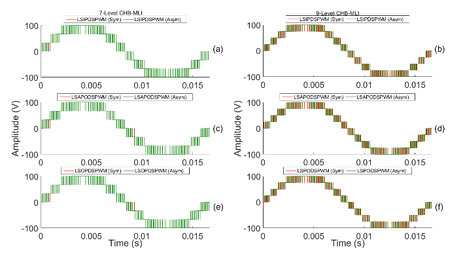
The output phase voltage (shown in Figure 16) formed by symmetric and their respective asymmetric design of CHB-MLIs using all LSSPWM method. The information implies both forms of CHB-MLIs results are equivalent to each other. Similarly, the waveform produced by symmetric and their respective asymmetric design of CHB-MLIs using all THILSPWM techniques is denoted in Figure 17. The statistics shows that both sorts of CHB-MLIs outputs are similar.
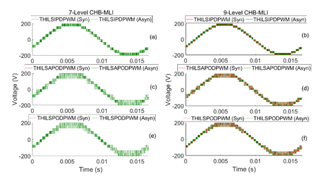
The L-L output voltage produced by symmetric and their respective asymmetric design of CHB-MLIs using all LSSPWM methos is shown in Figure 18. The numbers signify the output voltages are corresponding to each other for both designs of CHB-MLIs. Additionally, the L-L voltage waveform produced by symmetric and their corresponding asymmetric CHB-MLIs applying all THILSPWM method is shown in Figure 19. The results shows that both CHB-MLI’s outputs are like each other.
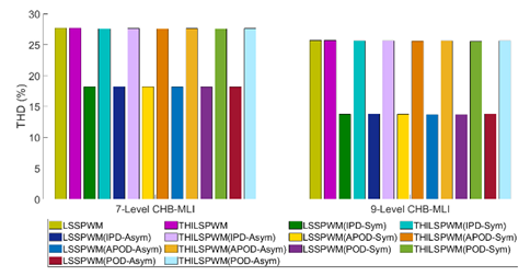
Figures 20 & 21 shows the THD results of the L-L voltages and phase-voltages waveform of 7- and 9-levels of symmetric/asymmetric design of CHB-MLI for all MCPWM methods, respectively.
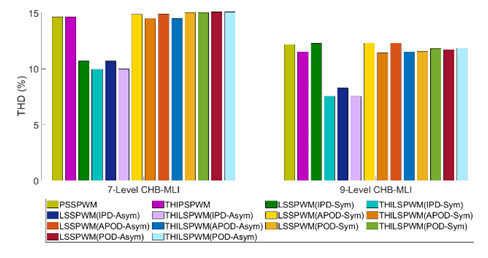
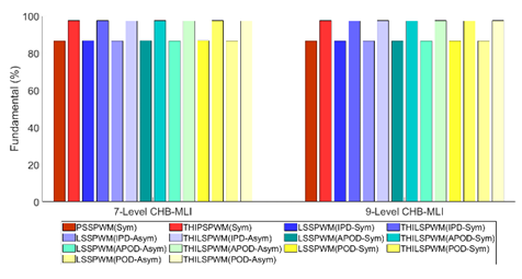
Figure 22 shows the fundamental component produced in the output voltage of 7- and 9-levels of both types of CHB-MLI for all MCPWM methods, correspondingly.
Additionally, the PSSPWM and THIPSPWM methods are employed to the 7- & 9-levels symmetrical CHB-MLI to confirm the discharging rate of the input HB sources. The discharging current of all inputs evaluated for PSPWM methods are equal. As depicted in Figure 23, discharging current from all sources in the THIPSPWM modulated CHB-MLI is a bit greater than the PSSPWM controlled CHB-MLI.
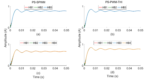
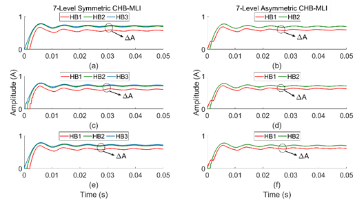
Also, the all deviations of LSSPWM and THILSPWM methods are applied to the 7- & 9-levels symmetrical and asymmetrical configuration of CHB-MLI to confirm the discharging of the input source of HB. The RMS value of discharging current of all sources are shown in Figures 24 to 27 ((a)-(f)). The calculated value show that variations of LSPWM method has discharging rate of rA difference. As described in Figures 26 and 27, discharging current of all inputs in the THILSPWM controlled CHB-MLI is slightly greater than the LSSPWM created CHB-MLI. Also, it has similar rA discharging difference in both symmetrical and asymmetrical type CHB-MLIs.
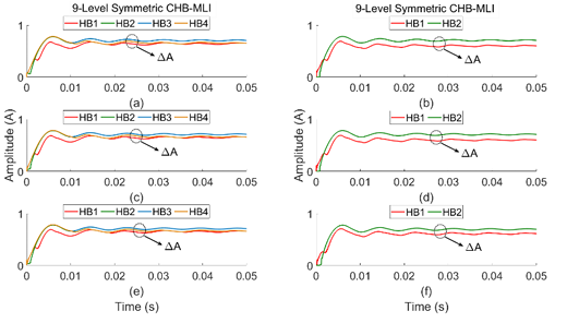
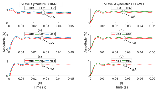
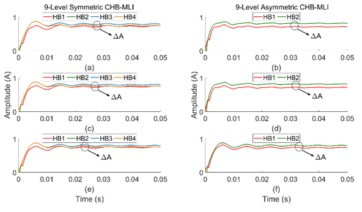
Table 1: Fundamental component and THD products of symmetrical CHB-MLI
PWM Methods | Symmetrical type (3-phase) | |||||
7-Level | 9-Level | |||||
N | THD (%) | F (%) | N | THD (%) | F (%) | |
PSSPWM | 36 | 14.65 | 86.60 | 48 | 12.19 | 86.60 |
THDPSPWM | 36 | 14.65 | 97.45 | 48 | 11.51 | 97.45 |
LSIPDSPWM | 36 | 10.72 | 86.75 | 48 | 12.29 | 86.60 |
THDLSIPDPWM | 36 | 9.97 | 97.55 | 48 | 7.56 | 97.40 |
LSAPODSPWM | 36 | 14.88 | 86.75 | 48 | 12.30 | 86.60 |
THILSAPODPWM | 36 | 14.49 | 97.55 | 48 | 11.44 | 97.40 |
LSPODSPWM | 36 | 15.05 | 86.75 | 48 | 11.57 | 86.60 |
THDLSPODPWM | 36 | 15.05 | 97.55 | 48 | 11.84 | 97.40 |
Table 2: Results of essential component and THD of symmetrical CHB-MLI
PWM Methods | Asymmetrical type (3-phase) | |||||
7-Level | 9-Level | |||||
N | THD (%) | F (%) | N | THD (%) | F (%) | |
LSIPDSPWM | 24 | 10.70 | 86.75 | 24 | 8.29 | 86.60 |
THILSIPDPWM | 24 | 10.01 | 97.55 | 24 | 7.56 | 97.40 |
LSAPODSPWM | 24 | 14.91 | 86.75 | 24 | 12.31 | 86.60 |
THILSAPODPWM | 24 | 14.53 | 97.55 | 24 | 11.51 | 97.40 |
LSPODSPWM | 24 | 15.10 | 86.75 | 24 | 11.74 | 86.60 |
THILS-PODPWM | 24 | 15.11 | 97.55 | 24 | 11.86 | 97.40 |
The fundamental component and THD are compared for both designs of CHB-MLIs which is summarized in Table 1 and Table 2. In these tables, “N” is the total number of switches used to compose CHB-MLIs. Also, the “F” value showed the essential component in the output signal.
Table 3: THD in the phase voltage of symmetrical CHB-MLI
PWM Methods | Symmetrical type (3-phase) | |||
7-Level | 9-Level | |||
N | THD (%) | N | THD (%) | |
PSSPWM | 36 | 27.67 | 48 | 25.61 |
THIPSPWM | 36 | 27.67 | 48 | 25.61 |
LSIPDSPWM | 36 | 18.16 | 48 | 13.77 |
THILSIPDPWM | 36 | 27.59 | 48 | 25.59 |
LSAPODSPWM | 36 | 18.16 | 48 | 13.74 |
THILSAPODPWM | 36 | 27.59 | 48 | 25.60 |
LSPODSPWM | 36 | 18.16 | 48 | 13.71 |
THILSPODPWM | 36 | 27.59 | 48 | 25.56 |
Tables 3 & 4 Summaries the THD generated in the phase voltage of the symmetrical/asymmetrical type 7& 9levels CHB-MLIs.
Table 4: THD in the phase-voltage of asymmetrical type CHB-MLI
PWM Methods | Asymmetrical type (3-phase) | |||
7-Level | 9-Level | |||
N | THD (%) | N | THD (%) | |
LSIPDSPWM | 24 | 18.21 | 24 | 13.78 |
THILSIPDPWM | 24 | 27.61 | 24 | 25.64 |
LSAPODSPWM | 24 | 18.20 | 24 | 13.71 |
THILSAPODPWM | 24 | 27.61 | 24 | 25.65 |
LSPODSPWM | 24 | 18.20 | 24 | 13.78 |
THILSPODPWM | 24 | 27.62 | 24 | 25.64 |
8. Conclusion
This paper analyzed MC-PWM techniques for the symmetric/asymmetric CHB-MLIs. A simulation model for a three-phase symmetric and asymmetric design of CHB-MLI was constructed in MATLAB. The operation of CHB-MLI was brought out at 5760 Hz, which is 96 times of fundamental (60 Hz) frequency inverter switching frequency.
This study discussed the structure of symmetrical and asymmetrical (binary and trinary) type CHB-MLI and the mathematical representation of their output voltages. The simulation results revealed that both types of converters generated equal “M” number levels in the output voltages using (M-1) carrier signals. However, the asymmetrical-trinary CHB-MLI needed the least number of switches and DC sources among symmetrical, asymmetrical (binary), and asymmetrical (trinary) configurations. Therefore, the asymmetrical-trinary configuration used fewer driver circuits, making it simpler, cost-effective, and less vulnerable. Also, the lowest number of switches in conduction per voltage level are needed in an asymmetrical-trinary configuration which shows that the conduction and switching losses are significantly lower leading to the higher efficiency of CHB-MLIs.
Finally, the simulation results revealed that the generated line-to-line and phase voltages by the 9-level (symmetrical and asymmetrical design) of CHB-MLI are much improved compared to the 7-level CHB-MLIs. In addition, it generated a high-quality voltage with the lowest harmonic content, which is 7.56% in line-to-line voltage and 13.71% in phase voltage. Even though, these harmonics are above the accepted limit of IEEE Std 519-1992, it minimizes the harmonic filtering process. That reduces the overall size and cost of the system.
Furthermore, this extensive study shows that the output signal produced by all MCPWM method is equivalent to a similar level of CHB-MLI. In addition, the harmonic study shows that the LSIPDPWM creates noticeably lower distortion (7.56% for 9-level inverter) in the L-L voltage compared to the other methods. The LSIPDPWM technique generated 13.78% THD in the phase-voltage for the 9-level CHB-MLI configuration. Moreover, the different arrangements of carrier signals have different THD in the output signal, which explains the arrangement of carrier signals impacts THD generation.
In addition, results reveal that LSTHIPWM produces nearly 10.8% additional fundamental components in the L-L voltage than the LSPWM, which improves the total productivity of CHB-MLI. That suggests the fundamental component produced in the output of CHB-MLI fit in with MC-design is affected by the choice of modulation signal.
Also, the measurement of source current displays that the PS-PWM technique can balance discharging current of all modules in CHB-MLI. In contrast, all variations of LSSPWM and THILSPWM do not naturally balance the discharging rate of all CHB-MLI modules. Therefore, the carrier rotation algorithm is needed with LSPWMs modulation techniques. This added algorithm increases the computation load on the digital controllers.

- M. H. Sree Reddy, N. Susheela, P. Malathy, “Sinusoidal tracking method for cascaded multilevel inverter fed induction motor drive,” 2021 Emerging Trends in Industry 4.0 (ETI 4.0), pp. 1–8, 2021, doi:10.1109/ETI4.051663.2021.9619306.
- M. Q. Kasim, R. F. Hassan, “Reduced computational burden model predictive current control of asymmetric stacked multi-level inverter based STATCOM,” 2021 IEEE International Conference on Automatic Control & Intelligent Systems (I2CACIS), pp. 374–379, 2021, doi:10.1109/I2CACIS52118.2021.9495881.
- E. Hallaji, H. M. Kojabadi, “Novel switched-capacitor-based multilevel inverter topology for renewable energy,” 2021 12th Power Electronics, Drive Systems, and Technologies Conference (PEDSTC), pp. 1–5, 2021, doi:10.1109/PEDSTC52094.2021.9405828.
- A. H. Hassanabad, D. Nazeipur, “Design and Simulation of a Control System for Investors in Wind Turbines,” vol. 6, no. 3, pp. 6, 2021.
- L. Mathe et al., “Battery pack state of charge balancing algorithm for cascaded H-Bridge multilevel converters,” 2016 IEEE 16th International Conference on Environment and Electrical Engineering (EEEIC), pp. 1–6, 2016, doi:10.1109/EEEIC.2016.7555737.
- A. Mittal, K. Janardhan, A. Ojha, “Multilevel inverter-based grid connected solar photovoltaic system with power flow control,” 2021 International Conference on Sustainable Energy and Future Electric Transportation (SEFET), pp. 1–6, 2021, doi:10.1109/SeFet48154.2021.9375753.
- H. Vahedi, A. Dehghanzadeh, K. Al-Haddad, “Static VAr compensator using packed U-cell based multilevel converter,” 2018 IEEE 12th International Conference on Compatibility, Power Electronics and Power Engineering (CPE-POWERENG 2018), pp. 1–5, 2018, doi:10.1109/CPE.2018.8372576.
- Z. Bayat et al., “Provide a new basic unit for cascaded multilevel inverter by reducing the maximum blocking voltage and switches,” 2019 27th Iranian Conference on Electrical Engineering (ICEE), pp. 576–581, 2019, doi:10.1109/IranianCEE.2019.8786387.
- X. Yuan, “Ultimate generalized multilevel converter topology,” IEEE Transactions on Power Electronics, vol. 36, no. 8, pp. 8634–8639, 2021, doi:10.1109/TPEL.2021.3056646.
- M. J. Uddin, Md. S. Islam, “Implementation of cascaded multilevel inverter with reduced number of components,” 2021 2nd International Conference on Robotics, Electrical and Signal Processing Techniques (ICREST), pp. 669–672, 2021, doi:10.1109/ICREST51555.2021.9331128.
- Z. E. Abdulhamed, A. H. Esuri, N. A. Abodhir, “New topology of asymmetrical nine-level cascaded hybrid bridge multilevel inverter,” 2021 IEEE 1st International Maghreb Meeting of the Conference on Sciences and Techniques of Automatic Control and Computer Engineering MI-STA, pp. 430–434, 2021, doi:10.1109/MI-STA52233.2021.9464511.
- W. Wan et al., “DC component self-balancing analysis of neutral-point in neutral-point-clamped three-level converters,” 2020 IEEE 9th International Power Electronics and Motion Control Conference (IPEMC2020-ECCE Asia), pp. 1752–1757, 2020, doi:10.1109/IPEMC-ECCEAsia48364.2020.9367804.
- N. K. Muthukuri, R. Tagore Yadlapalli, “Comparison of carrier based PWM technique for active neutral point clamping multilevel inverter,” 2020 4th International Conference on Intelligent Computing and Control Systems (ICICCS), pp. 1288–1292, 2020, doi:10.1109/ICICCS48265.2020.9121130.
- X. Jiang, M. L. Doumbia, “Comparative study of grid-connected multilevel inverters for high power phtovoltaic systems,” 2019 IEEE 7th International Conference on Smart Energy Grid Engineering (SEGE), pp. 184–190, 2019, doi:10.1109/SEGE.2019.8859784.
- A. Anthon et al., “Comparative evaluation of the loss and thermal performance of advanced three-level inverter topologies,” IEEE Transactions on Industry Applications, vol. 53, no. 2, pp. 1381–1389, 2017, doi:10.1109/TIA.2016.2639462.
- F. M. Shahir, E. Babaei, “16-level basic topology for cascaded multilevel inverters with reduced number of components,” IECON 2016 – 42nd Annual Conference of the IEEE Industrial Electronics Society, pp. 3105–3110, 2016, doi:10.1109/IECON.2016.7794068.
- A. S. Mohamad, N. Mariun, “Simulation of a 41-level inverter built by cascading two symmetric cascaded multilevel inverters,” 2016 7th IEEE Control and System Graduate Research Colloquium (ICSGRC), pp. 12–16, 2016, doi:10.1109/ICSGRC.2016.7813293.
- B. Rajesh, Manjesh, “Comparison of harmonics and THD suppression with three and 5 level multilevel inverter-cascaded H-bridge,” 2016 International Conference on Circuit, Power and Computing Technologies (ICCPCT), pp. 1–6, 2016, doi:10.1109/ICCPCT.2016.7530116.
- E. Babaei et al., “A new basic unit for symmetric and asymmetric cascaded multilevel inverter with reduced number of components,” IECON 2016 – 42nd Annual Conference of the IEEE Industrial Electronics Society, pp. 3147–3152, 2016, doi:10.1109/IECON.2016.7793089.
- L. Nanda, C. Jena, S. Samal, “Symmetrical and asymmetrical conventional cascaded multilevel inverter with SPWM technique,” 2021 International Conference on Intelligent Technologies (CONIT), pp. 1–5, 2021, doi:10.1109/CONIT51480.2021.9498417.
- A. Moeini, H. Iman-Eini, M. Najjar, “Non-equal DC link voltages in a cascaded H-bridge with a selective harmonic mitigation-PWM technique based on the fundamental switching frequency,” Journal of Power Electronics, vol. 17, no. 1, pp. 106–114, 2017, doi:10.6113/JPE.2017.17.1.106.
- O. V. Nos, E. E. Abramushkina, “The control technique for cascaded H-bridge multilevel converter with faulty cells,” 19th International Conference of Young Specialists on Micro/Nanotechnologies and Electron Devices (EDM), pp. 6403–6406, 2018, doi:10.1109/EDM.2018.8435054.
- N. Ramalingam, M. Saravanan, “Comparison of PWM control techniques for cascaded multilevel inverter,” International Review of Automatic Control (I.RE.A.CO), vol. 5, no. 6, pp. 815–828, 2012.
- A. R. Kumar et al., “A guide to nearest level modulation and selective harmonics elimination modulation scheme for multilevel inverters,” 2019 Innovations in Power and Advanced Computing Technologies (i-PACT), pp. 1–8, 2019, doi:10.1109/i-PACT44901.2019.8960205.
- A. Perez-Basante et al., “(2N+1) selective harmonic elimination-PWM for modular multilevel converters: A generalized formulation and a circulating current control method,” IEEE Transactions on Power Electronics, vol. 33, no. 1, pp. 802–818, 2018, doi:10.1109/TPEL.2017.2666847.
- Y. Deng, R. G. Harley, “Space-vector versus earest-level pulse width modulation for multilevel converters,” IEEE Transactions on Power Electronics, vol. 30, no. 6, pp. 2962–2974, 2015, doi:10.1109/TPEL.2014.2331687.
- Q. Liu et al., “A modified nearest-level modulation method for modular multilevel converter with fewer submodules,” 2017 Chinese Automation Congress (CAC), pp. 6551–6556, 2017, doi:10.1109/CAC.2017.8243957.
- R. B. Jonnala, N. R. Eluri, S. B. Choppavarapu, “Implementation, comparison and experimental verification of nearest vector control and nearest level control techniques for 27-level asymmetrical CHB multilevel inverter,” 2016 International Conference on Control, Instrumentation, Communication and Computational Technologies (ICCICCT), pp. 214–221, 2016, doi:10.1109/ICCICCT.2016.7987947.
- K. J. Pratheesh, G. Jagadanand, R. Ramchand, “A generalized-switch-matrix-based space vector modulation technique using the nearest level modulation concept for neutral-point-clamped multilevel inverters,” IEEE Transactions on Industrial Electronics, vol. 65, no. 6, pp. 4542–4552, 2018, doi:10.1109/TIE.2017.2772172.
- W. Abd Halim et al., “Selective harmonic elimination based on newton-raphson method for cascaded H-bridge multilevel inverter,” International Journal of Power Electronics and Drive Systems (IJPEDS), vol. 8, no. 3, pp. 1193, 2017, doi:10.11591/ijpeds.v8.i3.pp1193-1202.
- Y. Sinha, A. Nampally, “Modular multilevel converter modulation using fundamental switching selective harmonic elimination method,” 2016 IEEE International Conference on Renewable Energy Research and Applications (ICRERA), pp. 736–741, 2016, doi:10.1109/ICRERA.2016.7884431.
- M. Ye et al., “Research on current backflow of asymmetric CHB multilevel inverter,” Electronics, vol. 9, no. 2, pp. 214, 2020, doi:10.3390/electronics9020214.
- M. Moranchel et al., “Selective harmonic elimination modulation for medium voltage modular multilevel converter,” 2016 IEEE 7th International Symposium on Power Electronics for Distributed Generation Systems (PEDG), pp. 1–6, 2016, doi:10.1109/PEDG.2016.7527035.
- J. Bindu et al., “Genetic algorithm based selective harmonic elimination in PWM AC-AC converter,” 2011 International Conference on Recent Advancements in Electrical, Electronics and Control Engineering, pp. 393–397, 2011, doi:10.1109/ICONRAEeCE.2011.6129809.
- D. Ahmadi et al., “A universal selective harmonic elimination method for high-power inverters,” IEEE Transactions on Power Electronics, vol. 26, no. 10, pp. 2743–2752, 2011, doi:10.1109/TPEL.2011.2116042.
- M. S. A. Dahidah, G. Konstantinou, V. G. Agelidis, “A review of multilevel selective harmonic elimination PWM: formulations, solving algorithms, implementation and applications,” IEEE Transactions on Power Electronics, vol. 30, no. 8, pp. 4091–4106, 2015, doi:10.1109/TPEL.2014.2355226.
- C. Buccella et al., “A selective harmonic elimination method for five-level converters for distributed generation,” IEEE Journal of Emerging and Selected Topics in Power Electronics, vol. 5, no. 2, pp. 775–783, 2017, doi:10.1109/JESTPE.2017.2688726.
- H. Lin et al., “A flexible and fast space vector pulse width modulation technique for multilevel converters,” 2019 22nd International Conference on Electrical Machines and Systems (ICEMS), pp. 1–4, 2019, doi:10.1109/ICEMS.2019.8921982.
- A. Kumar, D. Chatterjee, “A survey on space vector pulse width modulation technique for a two-level inverter,” 2017 National Power Electronics Conference (NPEC), pp. 78–83, 2017, doi:10.1109/NPEC.2017.8310438.
- M. A. Hosseinzadeh et al., “Performance evaluation of cascaded H-bridge multilevel grid-connected converter with model predictive control technique,” 2019 IEEE International Conference on Industrial Technology (ICIT), pp. 1806–1811, 2019, doi:10.1109/ICIT.2019.8755160.
- I. Ahmed, V. B. Borghate, “Simplified space vector modulation technique for seven‐level cascaded H‐bridge inverter,” IET Power Electronics, vol. 7, no. 3, pp. 604–613, 2014, doi:10.1049/iet-pel.2013.0135.
- J. I. Leon et al., “The essential role and the continuous evolution of modulation techniques for voltage-source inverters in the past, present, and future power electronics,” IEEE Transactions on Industrial Electronics, vol. 63, no. 5, pp. 2688–2701, 2016, doi:10.1109/TIE.2016.2519321.
- P. Vijayarajan, A. Shunmugalatha, H. Habeebullah Sait, “Development of modified carrier based PWM scheme for single phase H-bridge inverter fed isolated wind–PV systems,” Solar Energy, vol. 126, pp. 208–219, 2016, doi:10.1016/j.solener.2015.12.026.
- K. Yodpradit, A. Pichetjamroen, N. Tcerakawanich, “An inverse-sinusoidal PWM technique to improve thermal performance of IGBT module,” 2018 IEEE Transportation Electrification Conference and Expo, Asia-Pacific (ITEC Asia-Pacific), pp. 1–7, 2018, doi:10.1109/ITEC-AP.2018.8433304.
- P. M. Lingom et al., “A single-carrier PWM method for multilevel converters,” 2019 IEEE 10th International Symposium on Power Electronics for Distributed Generation Systems (PEDG), pp. 122–127, 2019, doi:10.1109/PEDG.2019.8807453.
- C. R. Balamurugan et al., “Design of new multilevel inverter topology for various unipolar inverted sine carrier PWM strategies,” i-manager’s Journal on Embedded Systems, vol. 2, no. 4, pp. 37–43, 2014, doi:10.26634/jes.2.4.2806.
- R. Nandhakumar, S. Jeevananthan, “Inverted sine carrier pulse width modulation for fundamental fortification in DC-AC converters,” 2007 7th International Conference on Power Electronics and Drive Systems, pp. 1028–1034, 2007, doi:10.1109/PEDS.2007.4487830.
- A. S. Rahimi A Subki et al., “Comparative study of sinusoidal PWM and third harmonic injected PWM on three phase cascaded H-bridge multilevel inverter at various amplitude modulation indices,” 2018 IEEE PES Asia-Pacific Power and Energy Engineering Conference (APPEEC), pp. 520–525, 2018, doi:10.1109/APPEEC.2018.8566478.
- M. E. Tamasas et al., “Comparison of different third harmonic injected PWM strategies for 5-level diode clamped inverter,” 2017 IEEE Power and Energy Conference at Illinois (PECI), pp. 1–6, 2017, doi:10.1109/PECI.2017.7935718.
- T. M. Blooming, D. J. Carnovale, “Application of IEEE STD 519-1992 Harmonic Limits,” Conference Record of 2006 Annual Pulp and Paper Industry Technical Conference, pp. 1–9, 2006, doi:10.1109/PAPCON.2006.1673767.
- “IEEE Recommended practice and requirements for harmonic control in electric power systems.” IEEE.
- A. Aktaibi, M. A. Rahman, A. Razali, “A critical review of modulation techniques,” 19th Annual Newfoundland Electrical and Computer Eng. Conference (NECEC 2010), 2010.
- A. Dekka et al., “Evolution of topologies, modeling, control schemes, and applications of modular multilevel converters,” IEEE Journal of Emerging and Selected Topics in Power Electronics, vol. 5, no. 4, pp. 1631–1656, 2017, doi:10.1109/JESTPE.2017.2742938.
- Y. Li, Y. Wang, B. Q. Li, “Generalized theory of phase-shifted carrier PWM for cascaded H-bridge converters and modular multilevel converters,” IEEE Journal of Emerging and Selected Topics in Power Electronics, vol. 4, no. 2, pp. 589–605, 2016, doi:10.1109/JESTPE.2015.2476699.
- F. Patkar et al., “Performance comparison of symmetrical and asymmetrical six-phase open-end winding drives with carrier-based PWM,” 2017 6th International Conference on Electrical Engineering and Informatics (ICEEI), pp. 1–6, 2017, doi:10.1109/ICEEI.2017.8312446.
- M. Meraj et al., “Novel level shifted PWM technique for unequal and equal power sharing in quasi z-source cascaded multilevel inverter for PV systems,” IEEE Journal of Emerging and Selected Topics in Power Electronics, vol. 9, no. 1, pp. 937–948, 2021, doi:10.1109/JESTPE.2019.2952206.
- K. Thakre, K. B. Mohanty, “Performance improvement of multilevel inverter through trapezoidal triangular carrier based PWM,” 2015 International Conference on Energy, Power and Environment: Towards Sustainable Growth (ICEPE), pp. 1–6, 2015, doi:10.1109/EPETSG.2015.7510170.
- J. Patel, V. K. Sood, “Analysis of symmetric and asymmetric CHB-MLI using MC based SPWM and THI-PWM,” 2020 IEEE Electric Power and Energy Conference (EPEC), pp. 1–7, 2020, doi:10.1109/EPEC48502.2020.9320041.