Determining the Parameters of the Sine-Wave Filter Factors Affecting Filtration Quality
(This article belongs to the Special Issue on Special Issue on Multidisciplinary Sciences and Advanced Technology 2022 and the Section Electronic Engineering (EEE))
Export Citations
Cite
Mikhail, P. (2022). Determining the Parameters of the Sine-Wave Filter Factors Affecting Filtration Quality. Journal of Engineering Research and Sciences, 1(4), 127–136. https://doi.org/10.55708/js0104015
Pustovetov Mikhail. "Determining the Parameters of the Sine-Wave Filter Factors Affecting Filtration Quality." Journal of Engineering Research and Sciences 1, no. 4 (April 2022): 127–136. https://doi.org/10.55708/js0104015
P. Mikhail, "Determining the Parameters of the Sine-Wave Filter Factors Affecting Filtration Quality," Journal of Engineering Research and Sciences, vol. 1, no. 4, pp. 127–136, Apr. 2022, doi: 10.55708/js0104015.
The paper deals with proposals for the procedure of selecting the parameters of the sine-wave filter in case of increased voltage frequency (400—600 Hz) on the output of frequency converter, which is an element of power supply system. Author describes in article the structure of the power supply system for an unmanned underwater vehicle, which contains a sine-wave filter connected to frequency converter output. The system’s simulator has a block structure. As blocks previously developed computer models of electrical devices (transformer, autonomous voltage inverter, L-shaped filter, rectifier) are used. The subject of sine-wave filter output voltage quality and contribution to this of input voltage’s modulation index is also described at 100—200 Hz.
1. Introduction
Computer simulation today is one of the most popular and wide-spread information technologies used for the analysis and synthesis of technical systems, the consideration of electromagnetic, mechanical, thermal and other processes in them (sometimes under conditions that are difficult or impossible to apply to a real technical device). Computer simulation allows us to reduce the cost of devices development, reducing the materials and time consumption, but at the same time as above consider many different options of construction and modes. This allow specialists to recognize unsuccessful technical solutions before failure occurs or other negative impact during operation and apply acceptable methods to fix them at various stages of the device lifecycle.
For a contemporary electric drive based on frequency controlled AC motors and for a power supply systems (PSS) which include a frequency converter (FC), the problem of electromagnetic compatibility is one of the most ones due to the features of technology of voltage generation by pulsed converters based on semiconductor switches. The output voltage of pulsed converters is formed as a sequence of pulses of trapezoidal shapes. Every pulse has very steep fronts. Such a voltage contains a wide range of higher time harmonics. An additional losses of energy for all elements of the electric circuit from the FC output to the load occurs because of this. One way to reduce the influence of higher time harmonics is the EMC filters installation [1, 2] to suppress them. The sine-wave filter (SF) [3, 4] is one of filter types for FC output voltage.
Author should like to describe and gradually consider have applied by him procedure of the SF parameters selection for increased up to 400—600 Hz frequency of voltage. Proposed parameters selection procedure takes into account the possibility of operating the SF in the fundamental harmonic’s frequency range. On other hand, the subject of SF output voltage quality and factors contributes to it is interesting.
2. The Initial Data and Limitations
The authors of [5-10] articles propose description of the PSS used for powering unmanned underwater vehicles. Figure 1 presents an example of underwater vehicle MCC-3000 produced by LLC Marine Geo Service (Moscow, Russia). Underwater vehicle’s PSS contain (Figure 2): a source of balanced three line-to-line voltage of 380 V RMS value at 50 Hz frequency; FC structure contains a 3-phase input rectifier 1 (diodes D7 – D12), DC voltage link 1 ( Ld1 , Cd1 as an L-shaped filter) and a 3-phase two-level autonomous voltage inverter (AVI) pulse width modulated (PWM) output voltage with frequency control (diodes D1 – D6 and IGBT T1 – T6), the FC’s output voltage fundamental harmonic frequency is f1 = 400—600 Hz in steady-state operation; SF ( RLSF , LSF , CSF , RCSF as 3-phase L-shaped filter); 3-phase step-up transformer (PT1); cable-umbilical ( RC , LC , CC ); 3-phase step-down transformer (PT2); 3-phase rectifier 2 (diodes D13 – D18); DC voltage link 2 ( Ld2 , Cd2 as an L-shaped filter) and an equivalent load in the form of resistance Rload. The DC voltage link 2 and the rectifier 2 represent the head part of another FC, which also includes another AVI, from which the wide speed range frequency controlled electric drive of propellers based on 3-phase synchronous AC motors is powered. In Figure 2 instead of these electric drive and AVI the resistor Rload drawn.
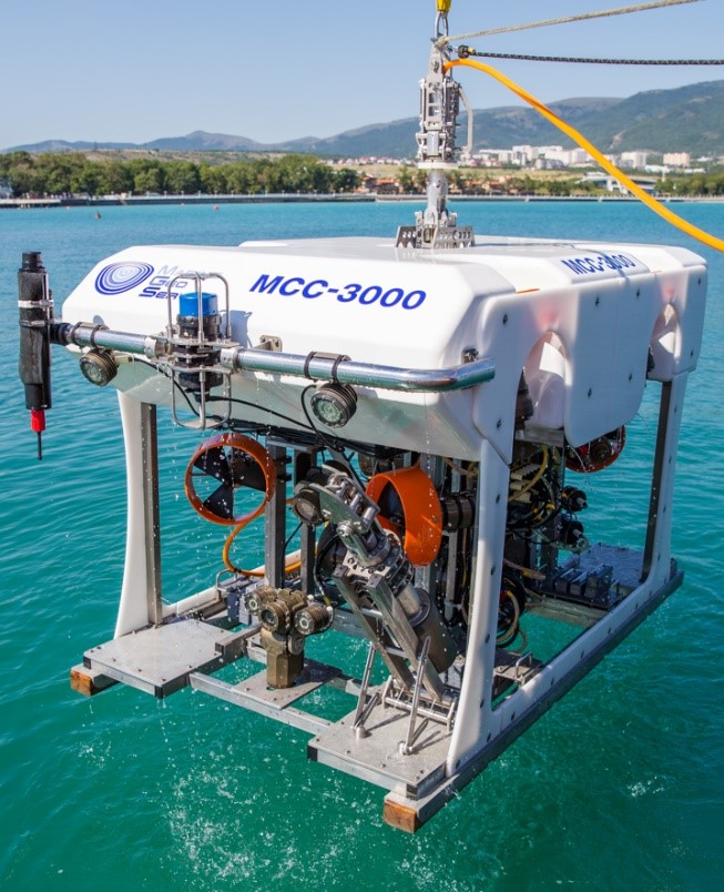
Marine Geo Service (Moscow, Russia)
fPWM = 14 kHz – is the PWM carrier frequency. The FC’s power is limited. That is the value of FC’s output current at long-term mode is limited. The same value IL∑ will have a current through inductance LSF of the SF phase. The LSF value is limited by the permissible voltage drop on it (percent impedance (short-circuit voltage vsc, %, equation (1))) caused by the current at long-term mode (for example, 10 % of the phase voltage fundamental harmonic RMS value). Needless to say, that FC’s output current IL∑ will contain wide harmonic spectrum. The voltage drop on the inductance caused by each current harmonic will be proportional to this harmonic frequency. Therefore, it is convenient to assume that the permissible voltage drop should occur from the flow through the inductor of only fundamental (first) current IL1 harmonic as a limitation for LSF calculations. The RMS value of the FC output current fundamental harmonic we can define through the usage of the power supplied by the primary 3-phase voltage source, the rated load power, the efficiency of devices (cables, transformers, rectifiers) series connected in the PSS. The resistance RLSF of the SF inductor phase LSF can be determined approximately in accordance with [1].
3. The Adopted Values for Parameters of Devices During Simulation
The SF of type Schaffner FN5020-75-35 parameters, being measured by the specialists of LLC Marine Geo Service (Moscow), in addition to the characteristics published in [11], are represented in Table 1, where Vp-p – the line-to-line voltage rated RMS value, f0 – the SF resonance frequency, Irated – the current through RLSF , LSF branch rated RMS value (FC rated output current).
$$v_{sc,\%} = \frac{\sqrt{3} I_{\text{rated}} \sqrt{(2 \pi f_1 L_{SF})^2 + R_{LSF}^2}}{V_{p-p}} \cdot 100\% \tag{1}$$
$$f_0 = \frac{1}{2 \pi \sqrt{L_{SF} C_{SFY}}}.\tag{2}$$
In equation (2) as CSFY we mean Y connection of SF phases capacitances. In case of Δ connection of capacitances will be true equation (3)
$$\begin{equation}
C_{SF\Delta} = \frac{C_{SFY}}{3}.
\end{equation}\tag{3}$$
For the cable-umbilical type KG (3×3,0+1×0,75+2x3E)-190-60 with a length of 3.4 km, based on its geometric dimensions, during simulation the parameters RC = 21.964 Ω , LC = 0.108 mH and CC = 0.168 µF have used. Author has used concentrated parameters for cable simulation. In accordance with data published in [6] it gives a slight discrepancy in the load voltage results compared to the model with distributed parameters (<6 %) and experimental data (within 5 %).
Both PT1 and PT2, which are part of the PSS, are constructed as a transformer group of three toroidal single-phase transformers inside the common protective shell. PT1 is the type OSM T 380/1900-12.0-400. PT2 is the type OSM T 1900/240-10.0-400. Each phase of PT1 and PT2 has a separate magnetic circuit. Because of this fact, a mathematical model of a 3-phase transformer without magnetic coupling between the phases (3 connected to each other models of single-phase transformer) has used. The approximate parameters of the T-shaped equivalent circuit of transformer [12] and characteristics used for the simulation of PT1 and PT2 are presented in Table 2. Magnetic saturation [13, 14] not taken into account.
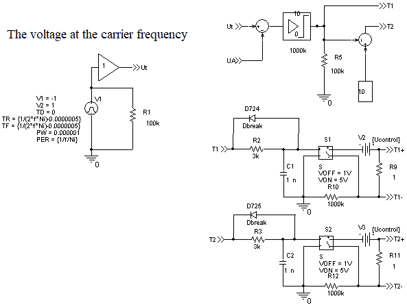
For the AVI simulation, the computer model based on idealized switches has used, similar to published in [1, 14], with the difference that in the control system had to reduce the capacitance of the capacitors from 10 nF (the value used in [1, 15] at fPWM = 1-2.5 kHz) to 1 nF at fPWM = 14 kHz (you can find C1 = C2 =1 nF in Figure 3).
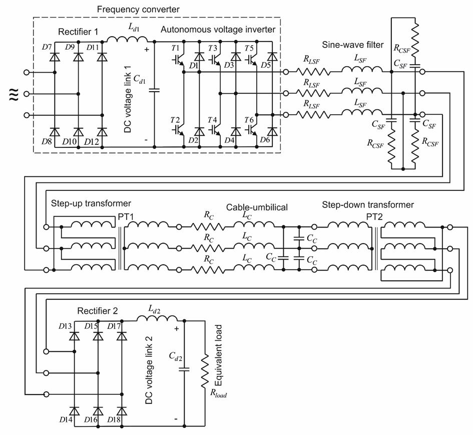
Table 1: Characteristics and Parameters of SF Type Schaffner FN5020-75-35
| f1 | Irated | Vp-p | LSF | RLSF | ||||
Hz | A | V | mH | mΩ | ||||
400 | 75 | 500 | 0.195 | 8.62 | ||||
600 | ||||||||
| CSF | RCSF | f0 | fPWM | $$\frac{f_{\mathrm{PWM}}}{f_0}$$ | vsc | |||
kHz | kHz | p.u. | % | |||||
8.5 | 10 | 2.3 | 14 | 6.2 | 13 | |||
19 | ||||||||
Table 2: Characteristics and Parameters for Simulation of 3-Phase Transformers
Name or symbol | Dimension | Value | ||||
for PT1 | for PT2 | |||||
T-shaped equivalent circuit parameters | Lσ1 | mH | 0.0191 | 1.286 | ||
| $$L’_{\sigma 2} = \left( \frac{w_1}{w_2} \right)^2 L_{\sigma 2} \approx \left( \frac{V_{1\,phase}}{V_{2\,phase}} \right)^2 L_{\sigma 2}$$ | ||||||
| r1 | mΩ | 5.7712 | 0.26 | |||
| r2 | 8.6567 | 0.173 | ||||
Connected in series | Lm | H | 0.0456 | 1.368 | ||
| rm | Ω | 21.83 | 654.875 | |||
The rated mode characteristics when powered by pure sinus voltage | V1phase – RMS value of primary winding phase voltage | V | 380 | 1900 | ||
V2phase – RMS value of secondary winding phase voltage | 1900 | 240 | ||||
Power on secondary winding terminals | kVA | 36 | 30 | |||
| f1 | Hz | 400 | ||||
Transformer’s current amplitude value at no load mode (close to magnetization current amplitude value at the rated mode) | A | 4.675 | 0.45 | |||
This shortens the pauses between switching off one and turning on the other switches at the same phase of the AVI model (for example, T2 and T1 in Figure 1a), and necessary to avoid the loss of short voltage pulses at the AVI output during simulation at high fPWM . The computer model of PSS implemented by means of PSpice [16-18]. For the DC voltage link simulation parameters of L-shaped filters shown in Table 3. These parameters determined according [15]. The load of the PSS (dissipates on Rload ) can vary from no-load mode to 45 kW overload. The rated power of PT1 is 36 kVA and 30 kVA for PT2.
4. The Suggested Sequence of Sine-Wave Filter Parameters Selection
- Let’s derive LSF from equation (1) on the base of permissible voltage drop caused by the IL1 . Generally recommended vsc, % = 10 %. may be neglected.
Table 3: Parameters values for L-shaped Filters of DC Voltage Links Simulation
| Ld1 | Ld2 | Cd1 | Cd2 |
mH | μF | ||
0.36 | 0.44 | 10700 | 9000 |
2. Set the frequency multiplicity \(\frac{f_{\mathrm{PWM}}}{f_0}\). For previously specified in this article fPWM and f1 values \(\frac{f_{\mathrm{PWM}}}{f_0}\) = 5 – 7 is suitable. Generally, the frequency multiplicity should be such that the AVI’s output voltage higher harmonic components caused by (they have high amplitudes) would be damped. After that let’s find .
3. Knowing LSF and f0 values we’ll derive from equation (2) the capacitance CSFY per phase of the SF if there is the Y connection. When there is the Δ connection we’ll find CSFΔ from equation (3).
Table 4: Bode Diagram for the SF of Type Schaffner FN5020-75-35
f , Hz | 400 | 2000 | 2800 | 600 | 3000 | 4200 | |
# of time harmonic | 1 | 5 | 7 | 1 | 5 | 7 | |
Output SF voltage/ input SF voltage, p.u. | at no load condition | 1.03 | 5.21 | 1.87 | 1.08 | 1.30 | 0.40 |
at rated load | 1.03 | 3.57 | 1.70 | 1.07 | 1.23 | 0.39 | |
Table 5: Simulation Results for the SF of Type Schaffner FN5020-75-35, Characterizing the Voltages Harmonic Composition
f , Hz | 400 | 2000 | 2800 | 600 | 3000 | 4200 |
Time harmonic’s # | 1 | 5 | 7 | 1 | 5 | 7 |
Output SF voltage/ input SF voltage, p.u. | 1.036 | 2.374 | 2.401 | 1.129 | 1.095 | 0.622 |
$$\frac{THD_{V_{outputSF}},\ \%}{THD_{V_{inputSF}},\ \%}$$ (taken into account HTH till 240 kHz) | $$\frac{6.017}{42.143}$$ | $$\frac{4.235}{45.232}$$ | ||||
4. Next step author suggests to provide simulation for checking the SF with previously calculated parameters for the absence in the f1 operating range of resonant phenomena associated with a significant increase in the filter’s output voltage amplitude. For this purpose, PSS’s simulator building recommended. Let’s make computational experiment fulfillment during which the FC’s output voltage and frequency firstly increases to a maximum value (ascending part of the graph 1 in Figures 4 and 5), followed by a steady state (horizontal part of graph 1), lastly at the fixed maximum output voltage of the AVI, the frequency is slowly reduced to the lower f1 boundary (the slope of the graph 1). Figures 4 and 5 use the following notation: 1 – graph of 2f1 , Hz; 2 – graph of SF’s output line-to-line instantaneous voltage. First of all, the computational experiment should be performed at no load condition – in this case, the resonant phenomena, if they exist, are manifested to the greatest extent. In addition, it is possible to perform the similar simulation under load. If resonant phenomena detected, to move them out of the frequency f1 operating range, it is appropriate to increase the inductance LSF. If this is not desirable, you can reduce the filter capacity CSF. We need to remember that for the same inductor reduction in capacity leads to a deterioration of filtering properties, and the increase in capacity, although approximating the shape of the filter’s output voltage to sinusoidal, but results to an increase of the current through the capacitance, including by increasing of the fundamental harmonic, and hence increase the SF’s inductor current, that is, FC’s output current, which can lead to overload and shutdown of the FC. Simultaneous increase of capacitance and inductance results to an increase in the denominator of the equation (2), that is, to f0 decrease and its shift toward f1 . This can cause the fundamental voltage harmonic amplification, which, under constant load, will lead to an increase in IL∑ and IL1 .
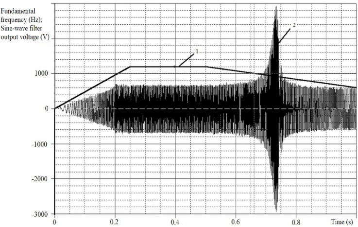
Figure 4: Results of simulation test for output voltage resonant phenomena in case of SF with LSF = 0.776 mH, CSFΔ = 20 μF and no load mode
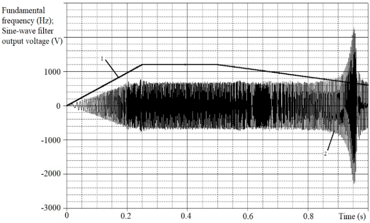
Figure 5: Results of simulation test for output voltage resonant phenomena in case of SF with LSF = 0.15 mH, CSFΔ = 20 μF and no-load mode
5. After all checking of the losses in the SF’s elements and the total power losses can be done. If the damping resistors in branches with capacitances are absent, we can estimate the series resistance connected with the phase capacitance of the order of units or tenths of (best – in accordance with the catalog data of capacitors). The focus on energy efficiency of equipment achievement, for example, in [19] is formulated as follows: “For two-level converters in the absence of various types of filters, these (additional due to non-sinusoidal supply voltage) losses can be … 1-2 % of the rated power of the motor. … there are losses in the filter, but they will be lower than the reduction of additional losses due to power from the converter. Thus, the total efficiency of the electric drive is increased.”
5. Justification of the Possibility of Increasing the Sine-Wave Filter’s Inductance Value
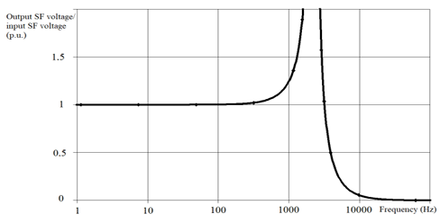
As we can see from Table 1, the SF type Schaffner FN5020-75-35 has vsc , % > 10 %. Let’s find out why this is allowed. In Figure 6 we can see the Bode diagram calculated for the SF type Schaffner FN5020-75-35. Table 4 contains the values of the same Bode diagram for some characteristic frequencies. From the Figure 6 and data Table 4 it follows that the SF voltage fundamental harmonic falls into the signal amplification region. One or both of the voltage’s lowest-frequency 5th and 7th highest time harmonics (HTH) also fall into there.
Bode diagram gives us a possibility to clarify the requirement to limit the voltage drop vsc , % in the SF’s phase inductor, which was limited to 10 % earlier, prohibiting voltage’s fundamental harmonic excessive weakening. Taking into account the SF output voltage’s fundamental harmonic gain, if necessary, we can assume vsc , % > 10 %, which has implemented for the SF type Schaffner FN5020-75-35 in accordance with Table 4 data.
6. Simulated Voltages for Different Blocks of PSS
The results of steady state mode voltages simulation for different blocks of the PSS under load with SF type Schaffner FN5020-75-35 we can see in Figure 7 and Figure 8. The following notation have adopted: 1 – line-to-line voltage at the FC output (SF input); 2 – phase-to- phase output voltage of SF; 3 – line-to-line voltage of the low voltage (secondary) winding of PT2; 4 – voltage on Cd2 and on Rload = 4.8 Ω ; 5 – rectifier 2 output voltage.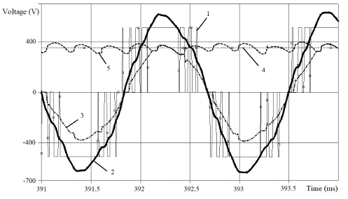
Figure 7: Simulated voltages for PSS at f1 = 600 Hz at 27.75 kW equivalent load
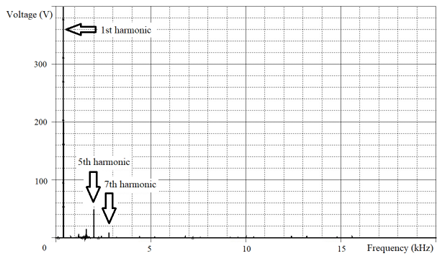
For the SF’s effectiveness demonstration Figure 9 and Figure 10 represent the spectral compositions of the line-to-line voltages at the SF’s input and output for the case shown in Figure 8.
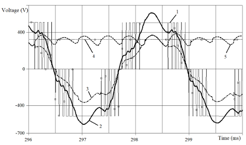
Figure 8: Simulated voltages for PSS at f1 = 400 Hz at 21.8 kW equivalent load
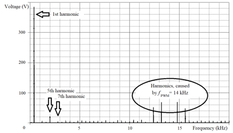
The comparison of Figure 9 and Figure 10 confirms that SF suppresses noticeably the HTH caused by fPWM , but, in accordance with Table 4 prediction, SF strengthens the 5th and 7th HTH, which causes the deformation of graphs 2 and 3 in Figure 8 especially. Also we can see that the voltage fundamental harmonic has amplified (Figure 10).
In Table 5 author summarize the processed results of Figure 7 and Figure 8 for the input and output line-to-line SF’s voltages. Needless to say, that results which Table 5 contains, in satisfactory agreement with the data of the Table 4 and Figure 6.
7. Impact Investigation of the DC Choke Ld2
We know, that the DC choke Ld2 may be absent in PSS. How does the voltage shape react to such a technical solution? In this case, the shape of voltages (graphs 2 and 3 in Figure 11, Figure 12) is close to pure sinus only at no load mode. While the load increases, the graph 2 shape deviates from the sine wave more and more. As we can understand from the harmonic analysis results, this occurs because of an increase of HTH with the 5th and 7th numbers in the voltage harmonic composition. At the same time, graph 3 will have flat (cut off) vertex.
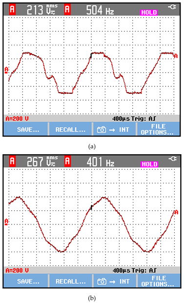
Furthermore, the absolute value of the amplitude of graph 3 (the flat vertex) coincides with the graph 4 parts. Simulation results in Figures 11 and 12 developed at LSF = 0.16 mH and CSFΔ = 13 μF. We can make a conclusion, that when the output rectifier 2 loaded directly by the capacitance, it is possible that SF will provide a close to pure sinus output voltage wave shape, but at no load mode only. In Figure 13 presented the confirmation of this conclusion by voltage waveforms of the experimental PSS (got by specialists of LLC Marine Geo Service (Moscow, Russia)).
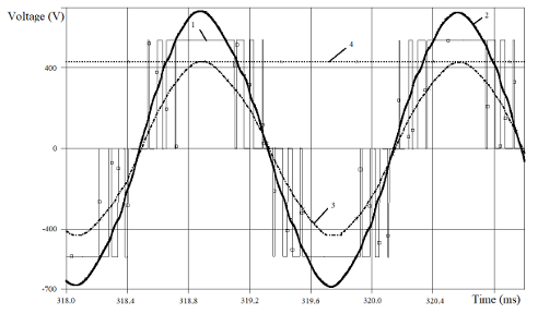
Figure 11: Simulated voltages for PSS without Ld2 at f1 = 600 Hz at no load mode
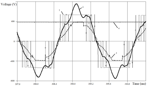
Figure 12: Simulated voltages for PSS without Ld2 at f1 = 600 Hz and 30.6 kW equivalent load value
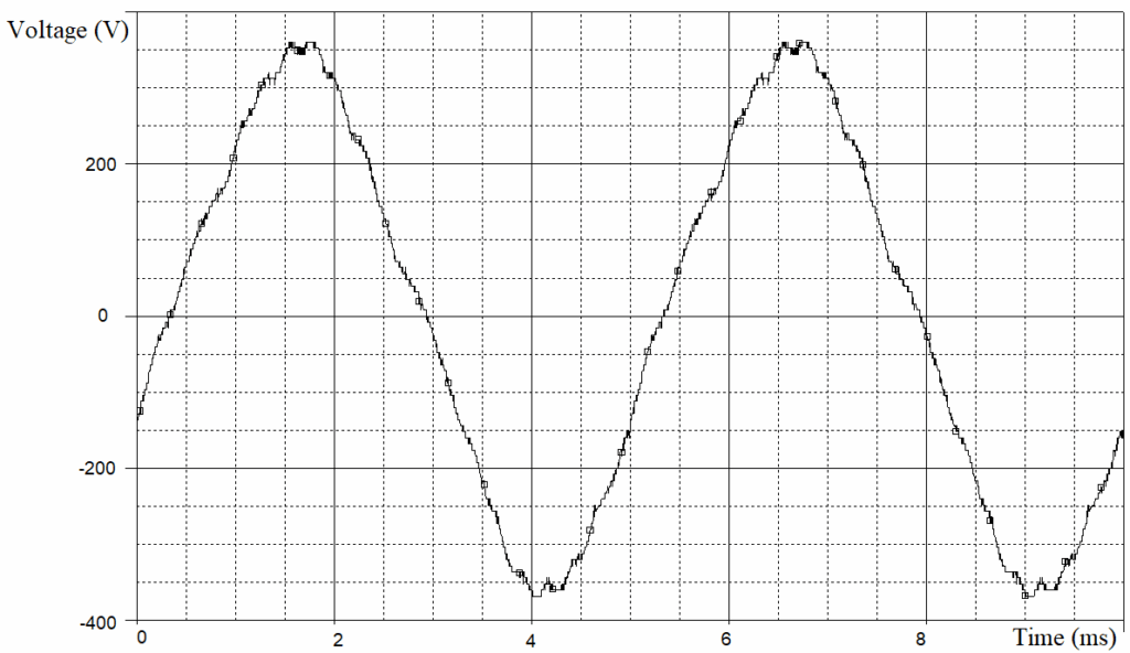
The experimental results in Figure 13 got for LSF = 0.09932 mH and CSFΔ = 12 μF at an equivalent load of 10 kW. Figure 13 (a) demonstrates the line-to-line voltage on the secondary winding of a step-down transformer PT2 at f1 = 504 Hz; (b) line-to-line SF output voltage at 401 Hz.
8. FC Output Voltage Modulation Index Contribution to SF Output Voltage Quality
Currently, FC with SF connected at the output are also used as a regulated power supply for testing electrical equipment [20, 21]. For example, for conducting experiments of open circuit (no load) and short circuit of power transformers.
It is known that the no-load test is carried out at the rated voltage. Otherwise the short-circuit test of the transformer is carried out at a reduced supply voltage in order to limit the currents through the windings. That is, the FC, for example, can form rated output line-to-line voltage of 690 V RMS. The same FC has to form output line-to-line voltage of 200 … 250 V RMS at the transformer short circuit test mode. This is 29 … 36% of the rated voltage (rounded to 1/3). This is actually the PWM modulation index, the duty cycle of the pulses averaged over the period of the modulating voltage. Therefore, 2/3 of the time in the voltage period is occupied by pauses (see in Figure 14 and Figure 15 the experimental graphs of line-to-line output voltage for the 3-phase FC of type GoodDrive GD300 (manufactured in China) with rated power of 1000 kW).
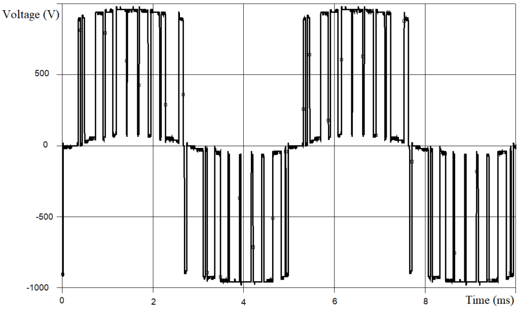
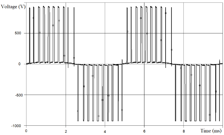
Figure 16 and Figure 17 show an experimental graphs of the line-to-line voltage at the SF’s output (SF equivalent parameters are LSF = 0.1 mH and CSFΔ = 240 μF (capacitances of SF phases connected in Δ scheme)). In all the experiments discussed in section 8 of this article, the PWM carrier frequency fPWM = 2 kHz.
Tables 6 and 7 show the results of harmonic analysis for the experimental graphs of line-to-line voltage at the FC output and at the SF output, respectively. In the tables 6 and 7 the HTH up to 1.6 MHz taken into account.
Test data for analysis provided by specialists of LLC Scientific and Production Enterprise “Electromash” (Novocherkassk, Russia).
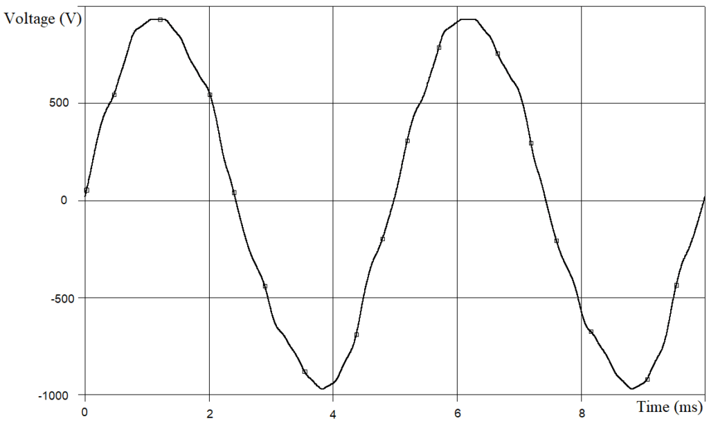
Table 6: THDVinputSF , % Depending on the RMS Value of 1st Harmonic Line-to-line Voltage Specified for the Inverter Output
Fundamental frequency f1 , Hz | RMS value of the 1st harmonic line-to-line voltage specified for the inverter output, V | THDVinputSF , % |
50 | 200 | 164.5 |
100 | 200 | 161.3 |
150 | 200 | 160.5 |
200 | 200 | 162.0 |
50 | 600 | 59.9 |
100 | 600 | 60.1 |
150 | 600 | 60.5 |
200 | 600 | 61.8 |
Table 7: THDVoutputSF , % Depending on the RMS Value of 1st Harmonic Line-to-line Voltage at the SF Output
Fundamental frequency f1 , Hz | RMS value of the 1st harmonic of line-to-line voltage at the SF output, V | THDVoutputSF , % |
100 | 260.4 | 8.5 |
200 | 239.1 | 8.0 |
100 | 662.2 | 5.0 |
200 | 663.9 | 5.7 |
9. Conclusion
Basing on predeveloped computer models of L-shaped filter, transformer, AVI, for which the necessary characteristics and parameters are defined and set, the simulator of PSS for an unmanned underwater vehicle has assembled. This computer model has got us an opportunity of electromagnetic processes simulation and studying at different power characteristics and loads. By means of simulation quantitatively and qualitatively has confirmed proper functioning of the SF of type Schaffner FN5020-75-35 in this PSS. This type of SF provides the sufficient filtering action and the resonant phenomena, which could lead to an output voltage’s significant increase, absence.
Author suggests provide simulation for checking the SF for absence of resonant phenomena, associated with a significant increase in the filter’s output voltage amplitude, within the f1
operating range. For this purpose, it is recommended computational experiment fulfillment in which, at first, FC’s output voltage and frequency increases to a maximum value, at second, a steady state follows, at third, the frequency is reduced slowly to the lower boundary at the fixed maximum AVI’s output voltage.
The Bode diagram usage gets an opportunity to refine the quantity requirement for the voltage drop limitation in SF’s phase inductor. Taking into account the gain of SF’s output voltage fundamental harmonic, if necessary, it is possible to assume vsc , % > 10 %.
When using SF loaded by rectifier, a simple way to minimize the SF’s output voltage distortion and voltage distortion at the terminals of an equivalent load over the wide range of load is an inclusion of DC choke Ld2 to DC voltage link 2 of PSS. In case of its absence, it is possible to achieve a sinusoidal SF’s output voltage shape only at no load mode. While load turned on, the SF’s output voltage and the voltage at load terminals shapes can have noticeable distortions. The Ld2 usage gives an additional positive effect, decreasing the voltage amplitude at the CSF terminals.
With a reduced value of the FC’s output voltage fundamental harmonic, as occurs in the short-circuit load mode, the harmonic composition of the FC output voltage is much more noisy than at no-load conditions, when the voltage of the fundamental harmonic of the FC is close to the rated value. That is, at a reduced voltage of the fundamental harmonic (low modulation index), the operating conditions of the SF are much more complicated than at the rated voltage of the fundamental. Namely: SF will, as expected, provide in the case of a reduced output voltage of the FC a worse harmonic composition of the voltage across the load than at the rated voltage of the FC.A particular problem arises if the SF must provide high-quality filtering over a wide range of output voltage values. This problem is further complicated if it is required to receive a voltage at the output of the inverter not of any one fixed frequency, but a certain range of voltage frequencies. In these conditions, it is practically impossible to cut out certain unwanted harmonics from the spectrum using passive filters without damaging the voltage waveform in any part of the regulated frequency range of the fundamental harmonic. Therefore, when formulating the requirements for the SF’s output voltage quality, it is advisable to clarify which mode of operation of the FC they correspond to, and whether an increase of voltage THDVoutputSF , % is permissible when deviating from this mode.
- M.Yu. Pustovetov, S.A. Voinash, “Analysis of dv/dt Filter Parameters Influence on its Characteristics. Filter Simulation Features,” 2019 International Conference on Industrial Engineering, Applications and Manufacturing (ICIEAM), pp. 1-8, 2019, doi:10.1109/ICIEAM.2019.8743007.
- C.F. Post, “EMC design considerations for medium to large variable speed drives in industry,” 2014 XXXIth URSI General Assembly and Scientific Symposium (URSI GASS), 2014, doi:10.1109/URSIGASS.2014.6929538.
- Baek Seunghoon, Choi Dongmin, Bu Hanyoung, Cho Younghoon 2020, “Analysis and Design of a Sine Wave Filter for GaN-Based Low-Voltage Variable Frequency Drives,” Electronics, vol. 9 (345), pp. 76-89, 2020, doi:10.3390/electronics9020345.
- E. Dresvianskii, M. Pokushko, A. Stupina, V. Panteleev, V. Yurdanova, “Control of high-voltage pump motor using a frequency sinewave filter converter,” IOP Conf. Ser.: Mater. Sci. Eng., vol. 450, p. 072003, 2018, doi:10.1088/1757-899X/450/7/072003.
- O. Sulaiman, A.H. Saharuddin, “Power Integrity Requirement of New Generation of ROV for Deep Sea Operation,” Global Journal of Researches in Engineering Automotive Engineering, vol. 12 (3), pp. 16-28, 2012.
- V.M. Rulevskiy, V.G. Bukreev, E.O. Kuleshova, E.B. Shandarova, S.M. Shandarov, Yu. Z. Vasilyeva, “The power supply system model of the process submersible device with AC power transmission over the cable-rope,” IOP Conf. Ser.: Mater. Sci. Eng., vol. 177 (1), p. 012098, 2017, doi:10.1088/1757-899X/177/1/012098.
- V.M. Rulevskiy, V.G. Bukreev, E.B. Shandarova, E.O. Kuleshova, S.M. Shandarov, Yu.Z. Vasilyeva “Mathematical model for the power supply system of an autonomous object with an AC power transmission over a cable rope,” IOP Conf. Ser.: Mater. Sci. Eng., vol. 177 (1), p. 012073, 2017, doi:10.1088/1757-899X/177/1/012073.
- V.M. Rulevskiy, V.A. Chekh, Y.A. Shurygin, A.A. Pravikova, “Voltage stabilizer in power supply of underwater vehicle,” IOP Conf. Ser.: Mater. Sci. Eng., vol. 327, p. 022018, 2018, doi:10.1088/1757-899X/327/2/022018.
- M.Yu. Pustovetov, “The Procedure of Sine-Wave Filter Parameters Selection Including Simulation in Case of Increased Frequency of Voltage,“ 2020 International Multi-Conference on Industrial Engineering and Modern Technologies (FarEastCon), 2020, doi:10.1109/FarEastCon50210.2020.9271606.
- V.М. Rulevskiy, A.A. Pravikova, D.Yu. Lyapunov, “Autonomous Inverters’ PWM Methods for Remotely Controlled Unmanned Underwater Vehicles,” 2016 International Conference on Industrial Engineering, Applications and Manufacturing (ICIEAM), 2016, doi:10.1109/ICIEAM.2016.7911641.
- Sine wave filters FN 5020 – SCHAFFNER Group – PDF Catalogs. https://pdf.directindustry.com/pdf/schaffner-group/sine-wave-filters-fn-5020/15134-878671.html
- M.Yu. Pustovetov, “A universal mathematical model of a three-phase transformer with a single magnetic core,” Russian Electrical Engineering, vol. 86 (2), pp.98-101, 2015, doi: 10.3103/S106837121502011X.
- M.Yu. Pustovetov, “Method for Taking into Account of Magnetization Curve Nonlinearity at Variable Frequency of Feeding Voltage,” 2018 International Conference on Industrial Engineering, Applications and Manufacturing (ICIEAM), 2018, doi:10.1109/ICIEAM.2018.8728613.
- M. Pustovetov, “An Inductive Coil Simulation,” International Journal of Power Systems, vol. 6, pp. 90-93, 2021
- M.Yu. Pustovetov, “Determination of the Sufficient Inductance of AC Line Reactor at the Input of Frequency Converter,” Journal of Modeling and Optimization, vol. 11 (1), pp. 25-29, 2019, doi:10.32732/jmo.2019.11.1.25.
- J. Keown, OrCAD PSpice and Circuit Analysis, Upper Saddle River: Prentice Hall, 2001.
- M.H. Rashid, SPICE for power electronics and electric power, CRC Press, 2012.
- A. Şchiop, V. Popescu, “PSpice simulation of power electronics circuit and induction motor drives,” Rev. Roum. Sci. Techn. – Électrotechn. et Énerg., vol. 52 (1), pp. 33–42, 2007.
- IEC TS 60034-25:2014 Rotating electrical machines — Part 25: AC electrical machines used in power drive systems — Application guide
- B. Leelachariyakul, P. Yutthagowith, “Resonant Power Frequency Converter and Application in High-Voltage and Partial Discharge Test of a Voltage Transformer,“ Energies, vol. 14, no. 7, p. 2014, 2021, doi:10.3390/en14072014.
- T. Prombud, P. Yutthagowith, “Development of High-voltage Testing System Based on Power Frequency Converter Used in Partial Discharge Tests of Potential Transformers,” Sensors and Materials, vol. 32, no. 2, pp. 573–585, 2020.